Photovoltaic Cells and Manufacture Method

a photovoltaic cell and manufacturing method technology, applied in the field of organic thin film photovoltaic cells, can solve the problems of high energy required for manufacture, high cost of materials, and insufficient cost of expensive devices, and achieve the effect of increasing the efficiency of photovoltaic conversion

Inactive Publication Date: 2009-04-02
HITACHI LTD
View PDF2 Cites 13 Cited by
  • Summary
  • Abstract
  • Description
  • Claims
  • Application Information

AI Technical Summary

Benefits of technology

[0014]The present invention has been made in view of these problems, and an object thereof is to provide photovoltaic cells and solar cells that stably increase photovoltaic conversion efficiency while restraining current leakage.
[0017]In accordance with the present invention, photovoltaic cells that stably increase photovoltaic conversion efficiency while restraining current leakage.

Problems solved by technology

However, those materials are costly, and an expensive device is necessary to carry out the procedures for manufacturing such solar cells.
Furthermore, the energy required for the manufacture is large, and it is difficult to restrict the power generation cost to about the same level as a general electricity expense.
In such circumstances, the future prospects are uncertain.
However, the dye-sensitized solar cells contain liquid electrolytes, and therefore, still have low reliability and stability.
To achieve high efficiency, expensive materials such as Ru-based dyes or platinum electrodes are necessary, and the production costs cannot be lowered.
If inexpensive materials are used, however, the conversion efficiency becomes much lower.
The problems with this structure are that the distance the excitons in the p-type semiconductor layer 7 can move is short, and the internal field layer is thin.
This results in insufficient light absorption, and high conversion efficiency cannot be achieved.
This leads to a decrease in conversion efficiency.
However, if the film thickness is small, light absorption becomes insufficient, and higher conversion efficiency cannot be expected.
As described above, organic semiconductors cannot be made thicker in general, having low carrier transport capability.
With organic semiconductors, there are the problems of insufficient light absorption, insufficient carrier generation, and decreases in efficiency.
However, it is easy to predict that a very long research and development period and enormous costs will be necessary.
However, thin-film defects are often caused in organic thin-film solar cells, and there is a large amount of leakage current in such organic thin-film solar cells.
Therefore, there is a high probability that recoupling is caused in the thin films.
Accordingly, if an organic thin film is formed on an electrode having a patterned indented interlayer, more defects are formed in the organic structure, and a larger amount of leakage current is generated than in a case where an organic thin film is formed on a smooth and flat substrate.
Therefore, the patterned indented interlayer is hardly maintained in the pn junction region, and it is difficult to achieve a desired effect.
However, if an organic thin film is deposited on the patterned indented surface arranged at longer intervals, a desired patterned indented interlayer cannot be formed in the photovoltaic conversion layer.

Method used


Image

  • Photovoltaic Cells and Manufacture Method
  • Photovoltaic Cells and Manufacture Method
  • Photovoltaic Cells and Manufacture Method

Examples


first embodiment

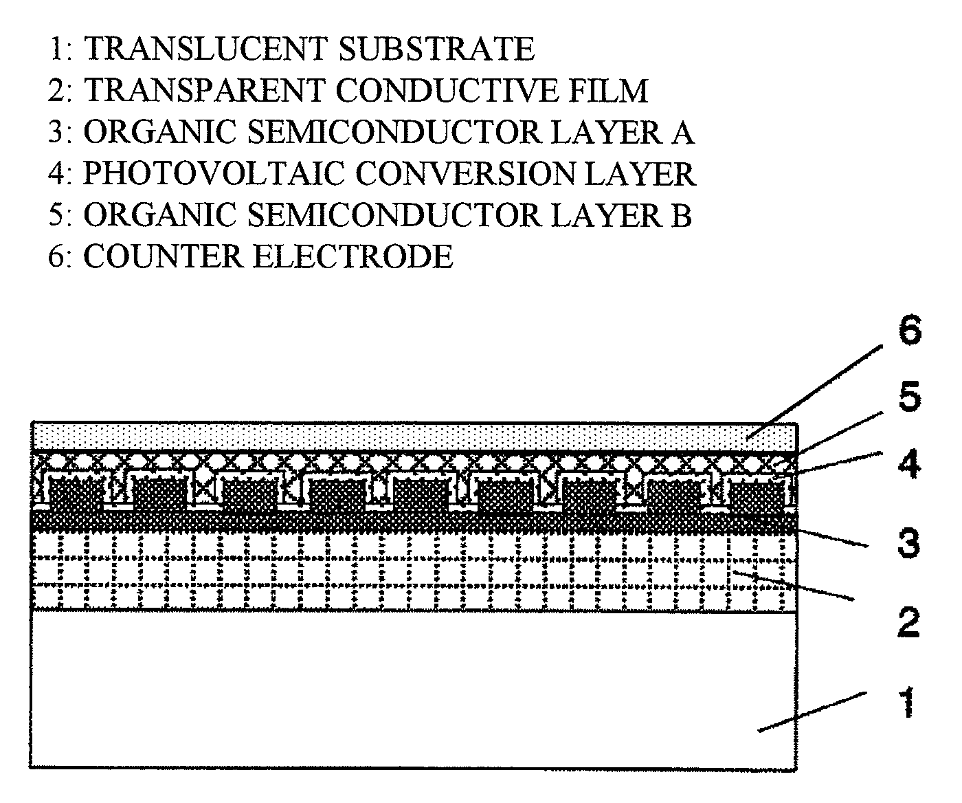
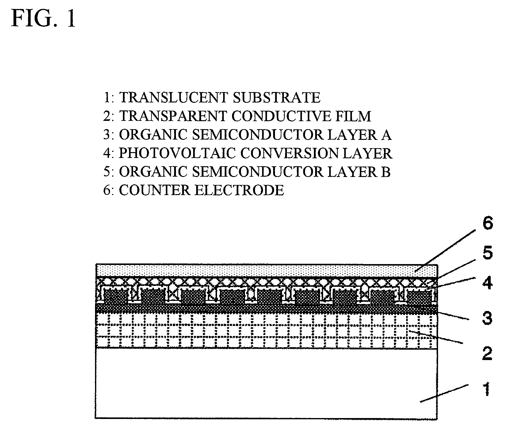
[0043]Next, embodiments of the present invention are described, (with reference to FIG. 1, whenever necessary).

[0044]A substrate electrode 1 is a translucent glass substrate formed by depositing ITO (indium tin oxide) as a transparent electrode (hereinafter referred to as the ITO substrate). The ITO substrate is subjected to ultrasonic cleaning with the use of a toluene solution, an acetone solution, and an ethanol solution for 10 to 15 minutes, respectively. The ITO substrate is then washed with pure water or ultrapure water, and is dried with a nitrogen gas.

[0045]An UV-ozone treatment is then carried out with the use of an UV irradiation device such as an ozone cleaner, so as to form a hydrophilic base on the substrate surface. In this manner, a hydrophilic substrate on which an organic semiconductor layer can be readily deposited is formed.

[0046]A mixed solution containing PEDOT / PSS to be a hole transport layer and ethylene glycol at the mixing ratio of 5:1 is applied by a spin c...

second embodiment

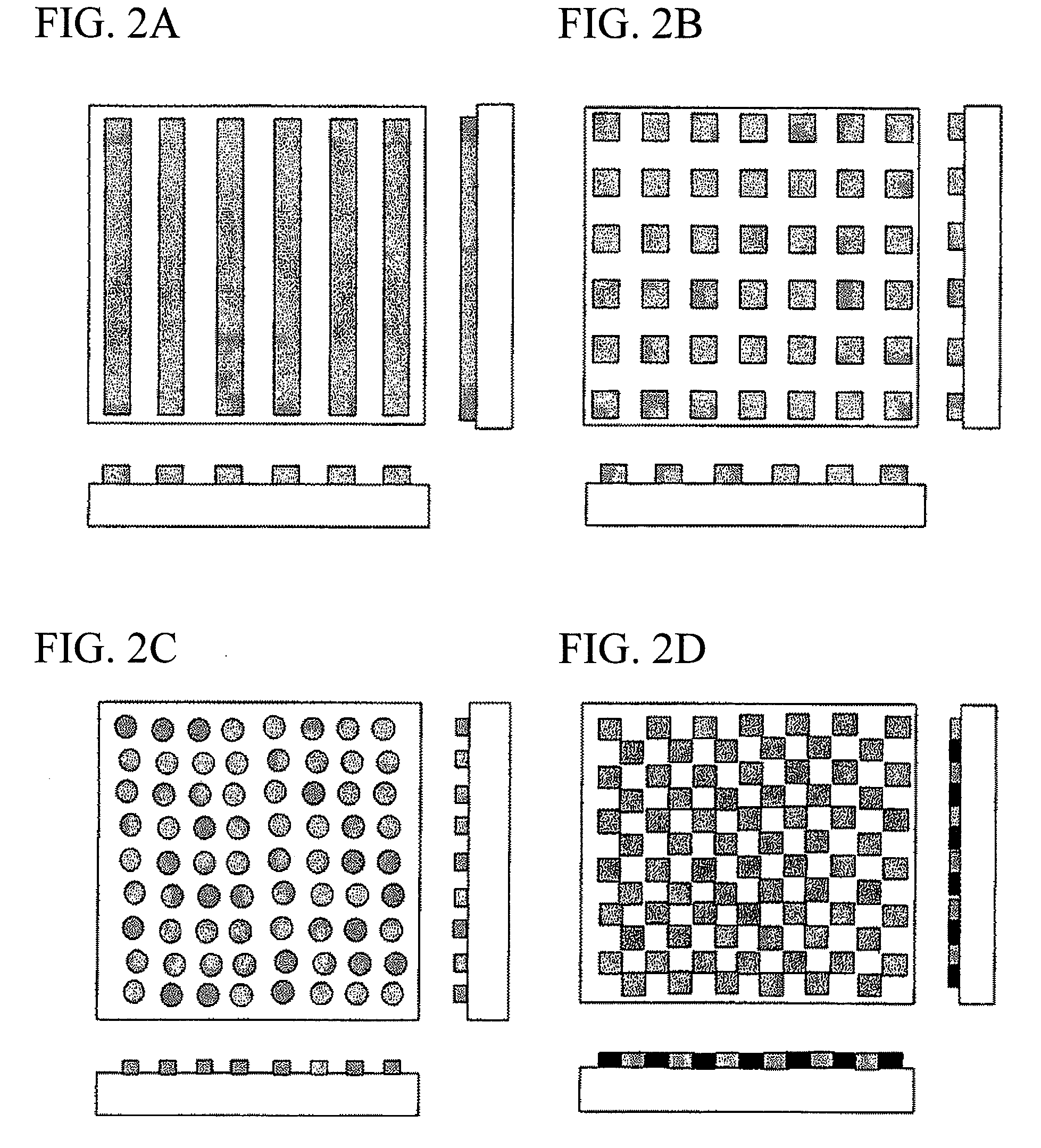
[0053]Photovoltaic cells are produced in the same manner as in the first embodiment, except that a nano-imprint metal mold having the indented pattern shown in FIG. 2A is used to form the patterned indented interlayer of the hole transport layer.

third embodiment

[0054]The photovoltaic conversion layer is formed by a simultaneous vapor deposition technique, instead of the thin film formation by the alternate adsorption technique used to form the photovoltaic conversion layer of the first embodiment. By the simultaneous vapor deposition technique, a p-type organic semiconductor film and an n-type organic semiconductor film are formed simultaneously through vacuum vapor deposition. Other than that, the same procedures as those of the first embodiment are carried out to form photovoltaic cells.


PUM

PropertyMeasurementUnit
distanceaaaaaaaaaa
contact angleaaaaaaaaaa
heightaaaaaaaaaa

Abstract

The present invention provides photovoltaic cells that stably increase photovoltaic conversion efficiency while restraining current leakage. The photovoltaic cells of the present invention include a transparent conductive layer formed on a light-permeable substrate, an organic semiconductor layer A covering the surface of the transparent conductive layer, a photovoltaic conversion layer in contact with the organic semiconductor layer, an organic semiconductor layer B in contact with the photovoltaic conversion layer, and a counter electrode in contact with the organic semiconductor layer B. In the photovoltaic cells, a patterned indented interlayer is formed at the interface between the organic semiconductor layer A and the photovoltaic conversion layer. With the patterned indented interlayer at the interface between the organic semiconductor layer A and the photovoltaic conversion layer, the interface between the organic semiconductor layer A and the photovoltaic conversion layer has a specific surface area 1.5 to 10 times as large as the interface between the transparent conductive layer and the organic semiconductor layer A.

Description

BACKGROUND OF THE INVENTION[0001]1. Field of the Invention[0002]The present invention relates to organic thin-film photovoltaic cells formed by stacking organic semiconductor layers, a photovoltaic conversion layer, and electrode layers, and more particularly, to photovoltaic cells that achieve high efficiency while maintaining high rectification, and a manufacture method for manufacturing the photovoltaic cells.[0003]2. Description of the Related Art[0004]Conventionally, solar cells of inorganic thin films made of Si, a GaAs compound, a CuInGaSe compound, or the like have been developed. However, those materials are costly, and an expensive device is necessary to carry out the procedures for manufacturing such solar cells. Furthermore, the energy required for the manufacture is large, and it is difficult to restrict the power generation cost to about the same level as a general electricity expense. In such circumstances, the future prospects are uncertain. To counter this problem, ...

Claims


Application Information

Patent Timeline
Patent Type & Authority Applications(United States)
IPC IPC(8): H01L31/0256H01L31/18
CPCB82Y10/00H01L51/0036H01L51/0037Y02E10/549H01L51/0047H01L51/424H01L51/447H01L51/0046Y02P70/50H10K85/1135H10K85/211H10K85/215H10K85/113H10K30/20H10K30/87
Inventor NAITO, HIROTOYOSHIMOTO, NAOKI
Owner HITACHI LTD
Why Eureka
Try Eureka