Method for producing multijunction solar cell

a solar cell and multi-junction technology, applied in the direction of semiconductor/solid-state device manufacturing, electrical apparatus, semiconductor devices, etc., can solve the problems of reducing crystal quality, and achieve the effect of increasing the area of the devi

Inactive Publication Date: 2009-04-02
HONDA MOTOR CO LTD
View PDF1 Cites 13 Cited by
  • Summary
  • Abstract
  • Description
  • Claims
  • Application Information

AI Technical Summary

Benefits of technology

[0014]An object of the present invention is to provide a method for producing a multijunction solar cell which can eliminate such a disadvantage to achieve a multijunction solar cell having four junctions and increase the area of a device.

Problems solved by technology

However, if such a procedure is employed, the semiconductor having a narrower band gap already grown in the shape of a wire will be deteriorated to reduce the crystal quality while the semiconductor having a wider band gap is growing in the shape of a wire.

Method used


Image

  • Method for producing multijunction solar cell
  • Method for producing multijunction solar cell
  • Method for producing multijunction solar cell

Examples


Embodiment Construction

[0039]Next, the embodiments of the present invention will be described in more detail with reference to the attached drawings.

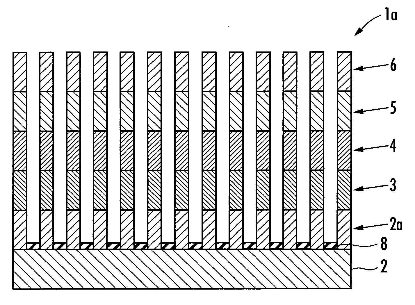
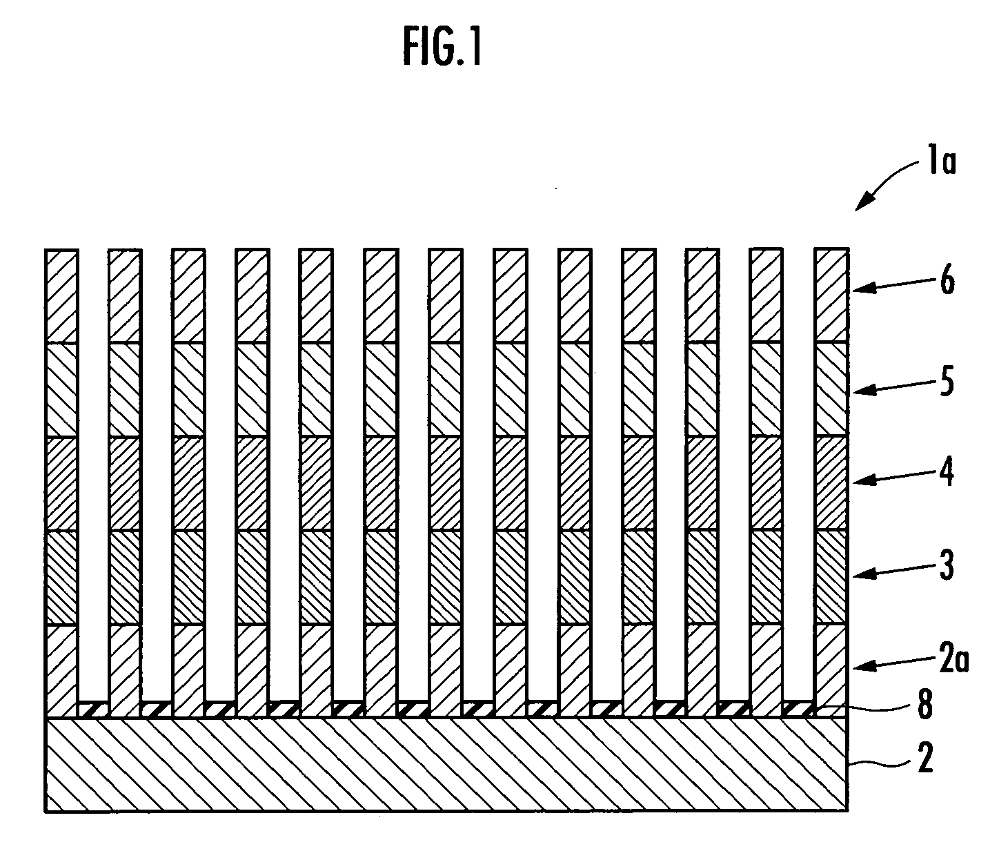
[0040]As shown in FIG. 1, a multifunction solar cell 1a obtained by the production method of the present embodiment comprises a substrate 2, a first semiconductor 2a grown in the shape of a wire on the substrate 2, a second semiconductor 3 which is connected to an end located farther from the substrate 2 of the first semiconductor 2a and is grown in the shape of a wire, a third semiconductor 4 which is connected to an end located farther from the substrate 2 of the second semiconductor 3 and is grown in the shape of a wire, a fourth semiconductor 5 which is connected to an end located farther from the substrate 2 of the third semiconductor 4 and is grown in the shape of a wire, and a fifth semiconductor 6 which is connected to an end located farther from the substrate 2 of the fourth semiconductor 5 and is grown in the shape of a wire. In the multijunction so...


PUM


Abstract

There is provided a method for producing a multijunction solar cell having four-junctions, the method allowing the area of a device to be increased. On a nucleation site formed on a substrate 2, is grown a semiconductor 2a comprising the same material as the substrate 2 in the shape of a wire. On the semiconductor 2a, are successively grown semiconductors 3, 4, 5, and 6 with a narrower band gap in the shape of a wire. The semiconductor 3 may be directly grown in the shape of a wire on the nucleation site formed on the substrate 2. It is preferred to form the nucleation site by forming an amorphous SiO2 coating 8a on the substrate 2 and etching a part of the amorphous SiO2 coating 8a. Further, it is preferred to form an insulating film 8 in the region except the nucleation sites on the substrate 2 by allowing the amorphous SiO2 coating 8a to remain therein. The semiconductor 2a is GaP; the semiconductor 3 is Al0.3Ga0.7As; the semiconductor 4 is GaAs; the semiconductor 5 is In0.3Ga0.7As; and the semiconductor 6 is In0.6Ga0.4As.

Description

BACKGROUND OF THE INVENTION[0001]1. Field of the Invention[0002]The present invention relates to a method for producing a multijunction solar cell.[0003]2. Description of the Related Art[0004]Conventionally, a single-junction solar cell comprising a single pn junction has been known. However, it is known that the power generation efficiency of the single-junction solar cell is only about 30% under terrestrial sunlight irradiation conditions irrespective of kind of semiconductor materials used, because the power generation efficiency has a theoretical limit determined by the band gap Eg of a semiconductor material used as a raw material.[0005]Thus, in order to obtain power generation efficiency higher than that of the single-junction solar cell, there is proposed a multijunction solar cell formed by laminating a plurality of solar cells in which each cell has a pn junction. As the simplest of the multijunction solar cells, there is known a two-junction solar cell 11 as shown in FIG. ...

Claims


Application Information

Patent Timeline
Patent Type & Authority Applications(United States)
IPC IPC(8): H01L31/0232
CPCH01L31/035281H01L31/03529Y02E10/544H01L31/1844H01L31/0687
Inventor GOTO, HAJIMEMOTOHISA, JUNICHIFUKUI, TAKASHI
Owner HONDA MOTOR CO LTD
Why Eureka
Try Eureka