Electronic Device Testing System and Method

a testing system and electronic device technology, applied in the direction of electric connection testing, measurement devices, instruments, etc., can solve the problems of high cost, inability to use aoi methods to examine pins, and only favorable mda for analog devices

Active Publication Date: 2009-04-02
TEST RES INC
View PDF8 Cites 16 Cited by
  • Summary
  • Abstract
  • Description
  • Claims
  • Application Information

AI Technical Summary

Benefits of technology

[0015]The testing system and method of present invention provides an examination of a DUT which electrically connects to a printed circuit board through the inner layer of the device. Particularly, the present invention provides a solution to the problems of HDI technology. The boundary-scan testing technology and the signal sensing unit are combined to deliver the tes

Problems solved by technology

However, AOI method can not be used to examine the pins, for example pins covered by the device itself such as in a “ball grid array” (BGA) packaged device.
Such problem can be resolved by using an “automatic X-ray inspection” (AXI); however the cost for such inspection is high.
However, MDA is only favorable for analog devices.
However, the complexity of printed circuit board assembly has increased significantly today, for example the number of pins is increased while the distance between the pins is decreased in devices such as CPU, ASIC, Chipset, etc.
Such complexity change reduces the number of possible testing points.
As the manufacturing process for semiconductor improves, the printed circuit board assembly, for example the ball grid array (B

Method used


Image

  • Electronic Device Testing System and Method
  • Electronic Device Testing System and Method
  • Electronic Device Testing System and Method

Examples


Embodiment Construction

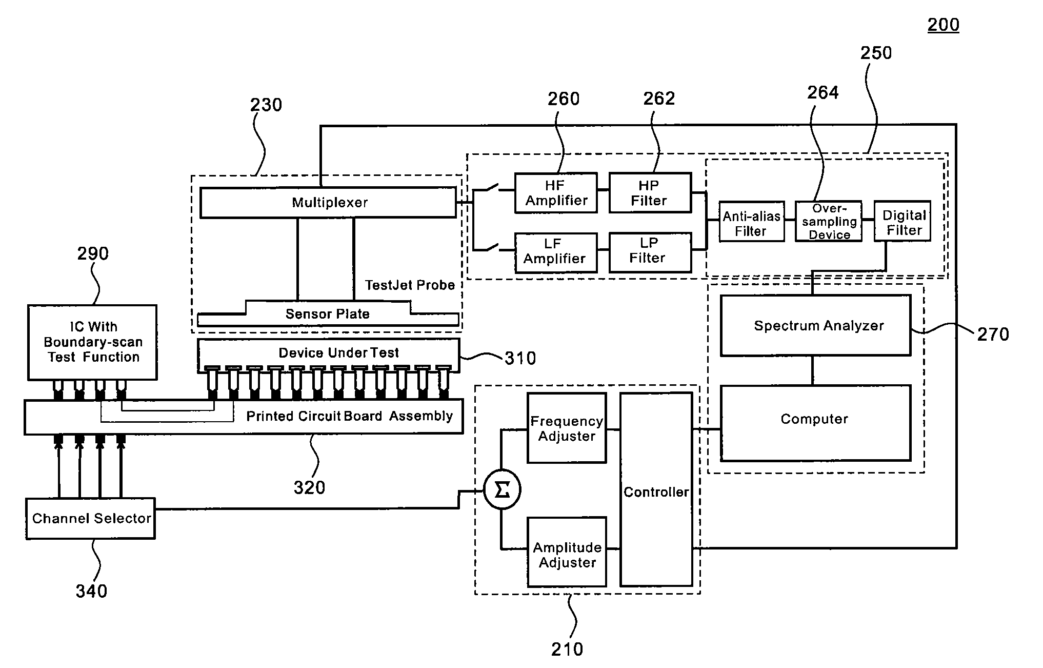
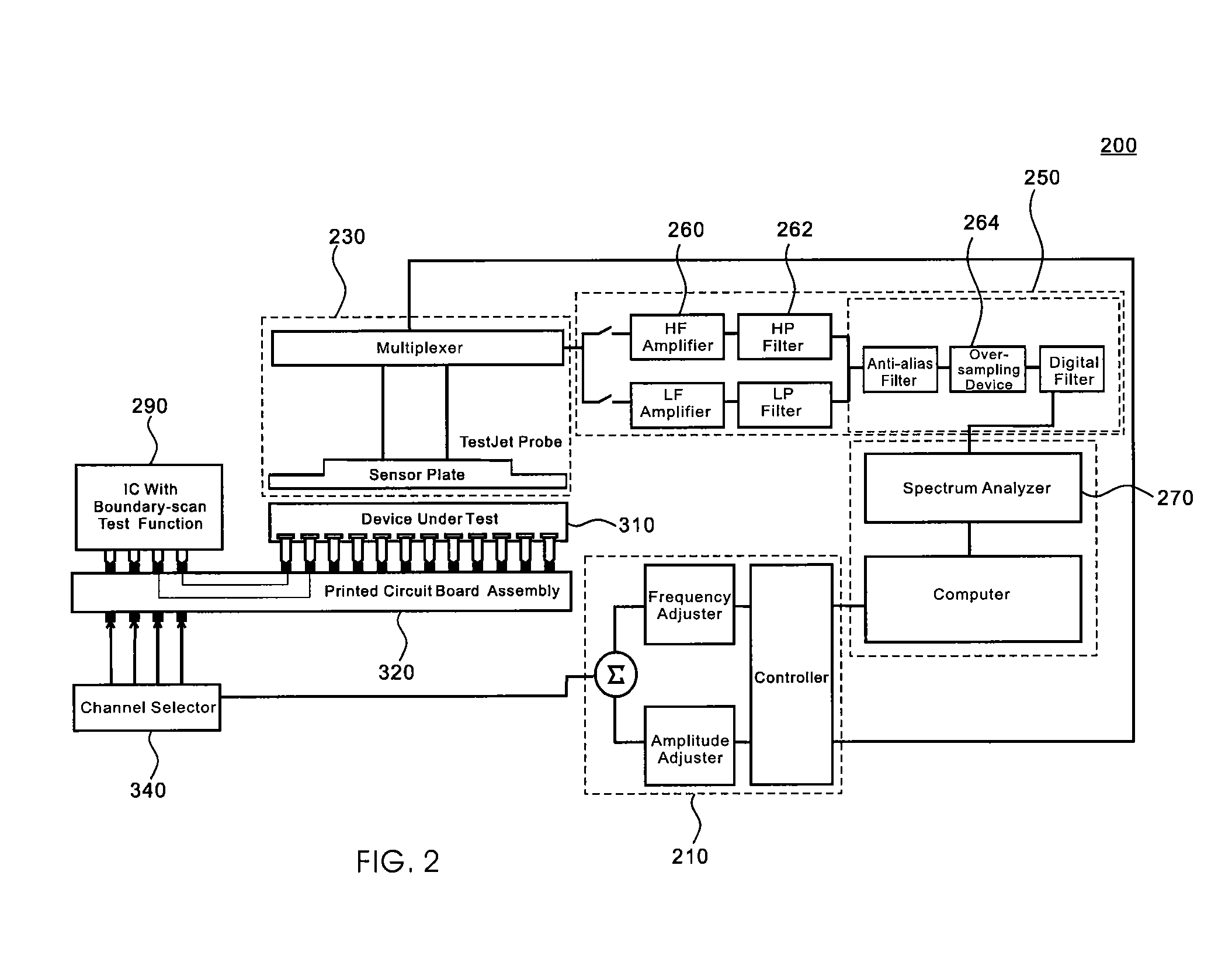
[0020]The present invention provides a system and method of inspection which can effectively examine whether the connection pins of DUT, for example an integrated circuit(IC), are properly connected to a printed circuit board assembly.

[0021]FIG. 2 shows a block diagram of the testing system of present invention. In this preferred embodiment, the testing system 200 comprises a testing signal source 210, a signal sensing unit 230, a signal processing unit 250, an analysis unit 270, and an IC with boundary-scan test function 290. The system 200 is capable of examining whether the pins of DUT 310(for example an IC) are properly connected to a printed circuit board assembly 320.

[0022]In one preferred embodiment, the testing signal source 210 which includes a controller, frequency adjuster and amplitude adjuster, outputs testing signals through a channel selector 340 to a IC with boundary-scan test function 290. The frequency of the testing signals can fall within the baseband of the expe...


PUM


Abstract

The invention provides a testing system and method suitable for determining whether a pin-out of an electrical component is properly connected to a PCB. The testing system includes a testing signal source, a signal detector, a signal processor, an analysis unit and an integrated circuit having boundary-scan test function to provide testing signals to the device under test (DUT) whose signal traces are passing through inner layer of PCB in order to detect whether the sensed signal is an error signal.

Description

FIELD OF INVENTION[0001]The present invention relates to a testing system and method, particularity relates to a system and method of examining whether the connection pins of a device under test (DUT) are properly connected with a printed circuit board assembly.BACKGROUND OF THE INVENTION[0002]The testing procedure of print circuit board assembly (PCBA), an important step in the front-end processes is examining whether the pins on integrated circuits (ICs), connectors and other electronic devices are properly connected to the printed circuit board. Such test not only can increase product quality, it can also detect manufacturing defects in the front-end processes. Today, the “automatic optical inspection” method (AOI) has replaced the conventional manual inspections. The AOI method not only reduces cost and eliminates human errors, but it also increases the speed of inspection. However, AOI method can not be used to examine the pins, for example pins covered by the device itself suc...

Claims


Application Information

Patent Timeline
IPC IPC(8): G01R31/28
CPCG01R31/046G01R31/70
Inventor CHEN, CHIA-MINGTSAI, SU-WEI
Owner TEST RES INC
Why Eureka
Try Eureka