

Sample surface observation method
a surface observation and sample technology, applied in the field of sample surface observation method, can solve the problems of resistance between the layers above and under the contact plug, and the detection of missing defects and open defects may be difficul
- Summary
- Abstract
- Description
- Claims
- Application Information
AI Technical Summary
Benefits of technology
Problems solved by technology
Method used
Image

Examples
Embodiment Construction
[0045]A description will now be given, with reference to the drawings, of an embodiment of the present invention.
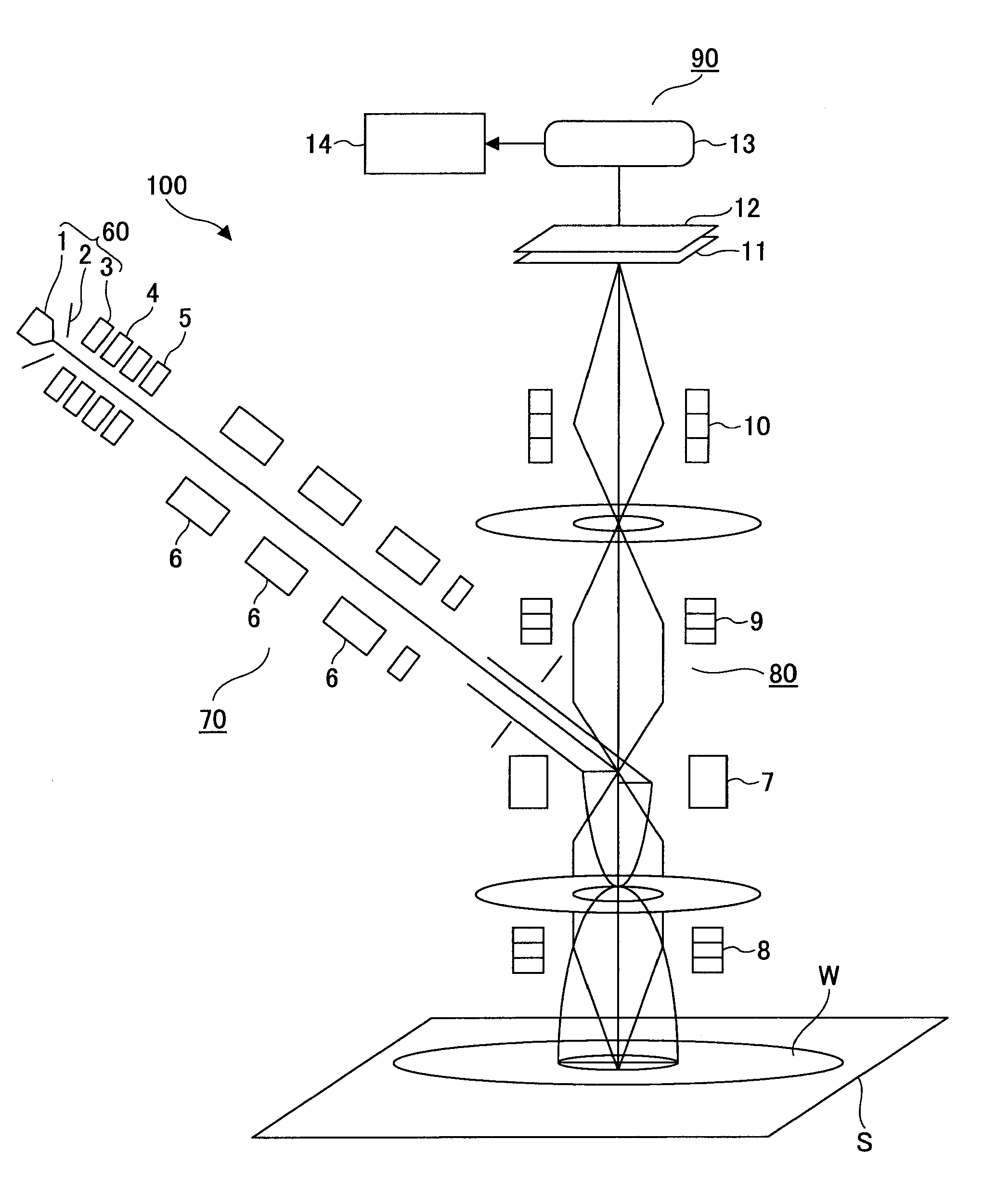
[0046]FIG. 3 is an illustration of an electron beam apparatus 100, which performs a test surface observation method according to an embodiment of the present invention. In FIG. 3, the electron beam apparatus 100 is equipped with an electron beam projection part 60, a primary electron optical system 70, a secondary electron optical system 80 and an electronic detection part 90.
[0047]The electronic beam projection part 60 is means for generating and projecting an electron beam. The electron beam projection part 60 is equipped with an electron gun 1, a Wehnelt electrode 2 and an anode 3. An electron beam emitted from a cathode electrode (not shown in the figure) of the electron gun 1 is controlled in its amount of emitted electrons by the Wehnelt electrode 2, and is accelerated by the anode 3 and enters the primary electron optical system 70.
[0048]The primary electron optica...
PUM
| Property | Measurement | Unit |
|---|---|---|
| landing energy | aaaaa | aaaaa |
| landing energy | aaaaa | aaaaa |
| landing energy | aaaaa | aaaaa |
Abstract
Description
Claims
Application Information