Electrochemical device

a technology of electrochemical devices and chips, applied in the direction of instruments, antenna supports/mountings, antennas, etc., can solve the problems of limiting the ability to mass-produce the tags to lower prices, difficult and expensive (>0.50 usd) manufacturing, and the chips used in prior art devices suffer from a lack of environmental friendliness, processability and economic production possibilities

Inactive Publication Date: 2009-04-09
KUGLER THOMAS +5
View PDF7 Cites 17 Cited by
  • Summary
  • Abstract
  • Description
  • Claims
  • Application Information

AI Technical Summary

Benefits of technology

[0010]Yet another object of the present invention is to provide an environmentally safe, capacitively coupled identification device with an active antenna logic connection so that the disposal of the device, along with any support onto which it has been deposited, does not give rise to handling problems, and so that no safety restrictions have to be imposed on the use of the device.
[0028]Thus, the bi-stable transistor embodiment of the present invention offers a memory function, in that it is possible to switch it on or off using only a short voltage pulse applied to the gate electrode. The transistor stays in the conducting or non-conducting redox state even after the applied voltage has been removed. A further advantage with such bi-stable transistors is that close to zero-power operation is made possible, since the short voltage pulses applied to the gate need not be larger than a fraction of the gate voltages needed for operation of a corresponding dynamic device.

Problems solved by technology

Problems with capacitively coupled identification devices in the prior art include that they are difficult and expensive (>0.50 USD) to manufacture.
In particular, the chip part of the identification unit is limiting the capability to mass-produce the tags to lower prices.
Furthermore, materials used in the chips of prior art devices suffer from a lack of environmental friendliness, processability and economic production possibilities.

Method used


Image

  • Electrochemical device
  • Electrochemical device
  • Electrochemical device

Examples


Embodiment Construction

Definitions

[0044]Bi-stable electrochemical transistor: an electrochemical transistor device in which the transistor channel retains its redox state (and hence its conductivity characteristics) when the gate voltage is removed.

[0045]Dynamic electrochemical transistor: an electrochemical transistor device in which the transistor channel spontaneously returns to its initial redox state (and hence to its initial conductivity characteristics) when the gate voltage is removed.

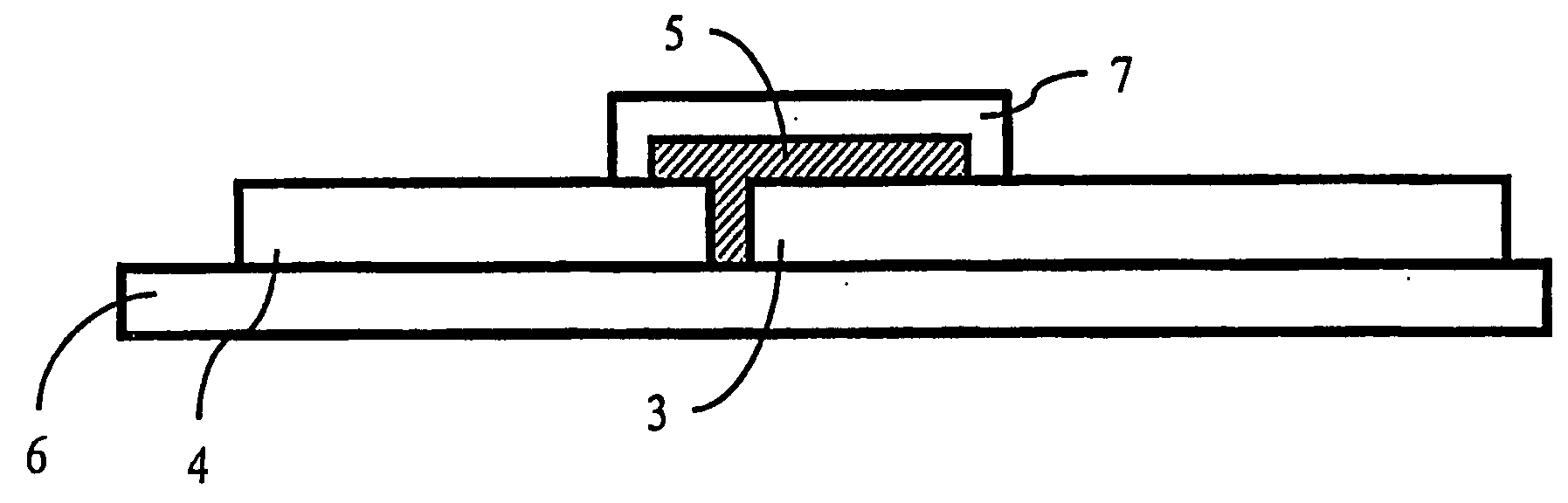
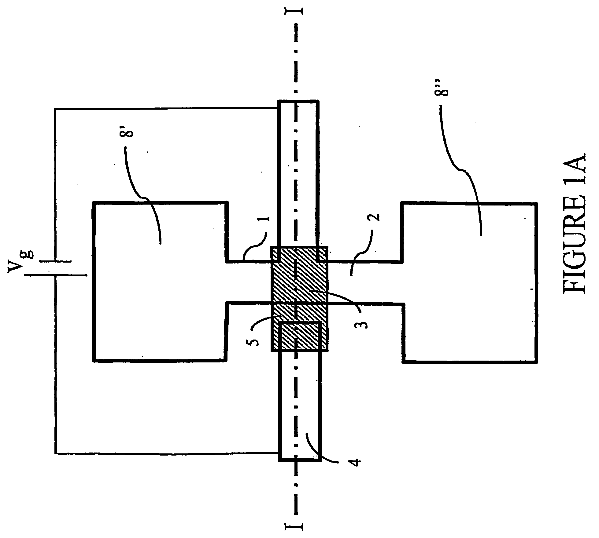
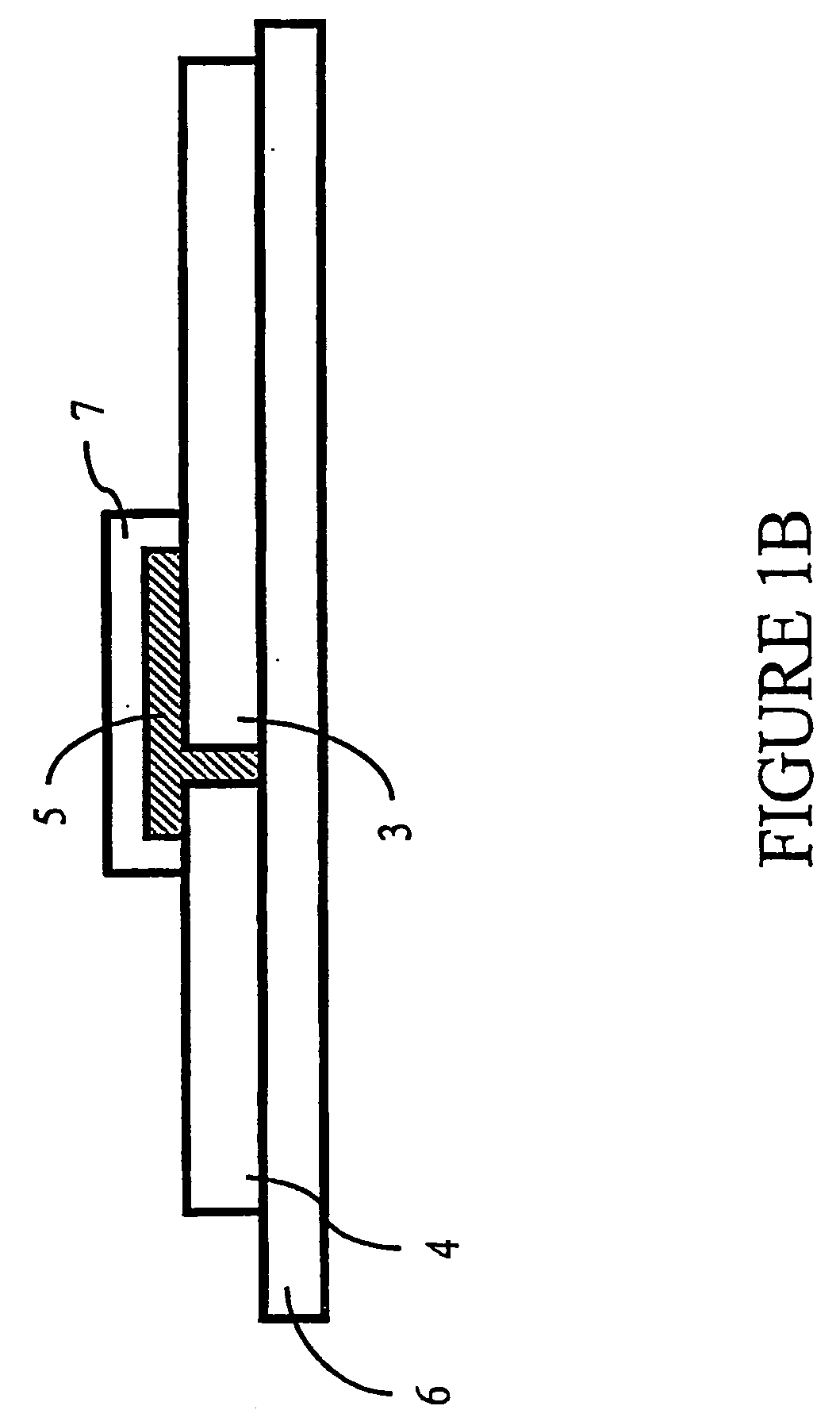
[0046]Source contact: An electrical contact that provides charge carriers to a transistor channel. According to the present invention, the source contact is connected to one of the pads of a capacitively coupled device (i.e. the first pad of the antenna member).

[0047]Drain contact: An electrical contact that accepts charge carriers from a transistor channel. According to the present invention, the drain contact is connected to one of the plates of an capacitive coupled device or coupled to ground (i.e. the second pad...


PUM

PropertyMeasurementUnit
thicknessaaaaaaaaaa
thicknessaaaaaaaaaa
widthaaaaaaaaaa

Abstract

An electrochemical device is provided, comprising a source contact connected to a first antenna pad, a drain contact connected to a second antenna pad, at least one gate electrode, an electrochemically active element arranged between, and in direct electrical contact with, the source and drain contacts, which electrochemically active element comprises a transistor channel and is of a material comprising an organic material having the ability of electrochemically altering its conductivity through change of redox state thereof, and a solidified electrolyte in direct electrical contact with the electrochemically active element and the at least one gate electrode and interposed between them in such a way that electron flow between the electrochemically active element and the gate electrode(s) is prevented. In the device, flow of electrons between source contact and drain contact is controllable by means of a voltage applied to the gate electrode(s).

Description

PRIORITY STATEMENT[0001]This is a continuation of U.S. application Ser. No. 10 / 495,653, filed Aug. 18, 2004, the entire contents of which are hereby incorporated by reference. This application claims the benefit of PCT Application No. PCT / SE02 / 0221, filed Nov. 29, 2002, the entire contents of which are hereby incorporated herein by reference.FIELD OF THE INVENTION[0002]The present invention relates to radio frequency identification tags, and in particular to a radio frequency identification tag that is modulated by an electrochemical device. In particular, the present invention relates to printable, electrostatic antennas together with printable electrochemical transistor devices, based on conducting organic and / or inorganic materials.BACKGROUND OF THE INVENTION[0003]Remotely read identification tags have a wide range of different applications and uses (see for example RFID HANDBOOK “Radio-Frequency Identification Fundamentals and Applications” by Klaus Finkenzeller, John Wiley & So...

Claims


Application Information

Patent Timeline
Patent Type & Authority Applications(United States)
IPC IPC(8): H01L51/10H01L51/40H01L51/05H01L29/76H01L29/786H01L51/00H01L51/30H01Q1/22H01Q23/00
CPCG06K19/027H01L51/0037H01Q1/2225H01L51/0512H01Q1/22H01L51/0508H10K85/1135H10K10/46H10K10/462
Inventor KUGLER, THOMASBERGGREN, MAGNUSREMONEN, TOMMIMALMSTROM, ANNA INGALILLKNUTHAMMAR, BJORNNORBERG, PETRONELLA
Owner KUGLER THOMAS
Why Eureka
Try Eureka