

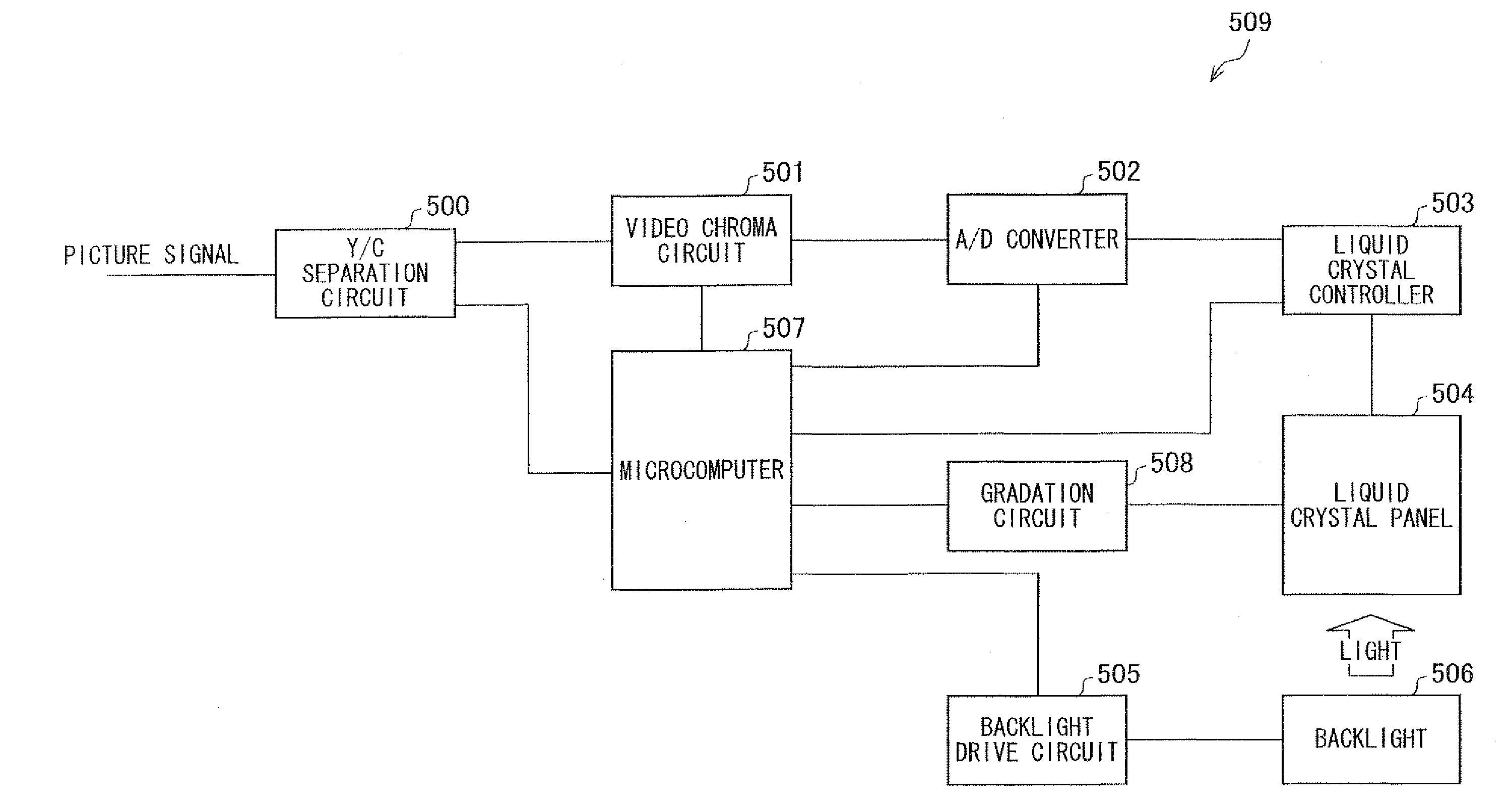
Active matrix substrate, display device, and television receiver
a technology of active matrix substrate and display device, which is applied in the direction of semiconductor devices, instruments, electrical apparatus, etc., can solve the problems of short circuit between drain lead-out electrodes, inability to avoid over-etching, and short circuit between drain leads, so as to improve transistor characteristics
- Summary
- Abstract
- Description
- Claims
- Application Information
AI Technical Summary
Benefits of technology
Problems solved by technology
Method used
Image

Examples
first embodiment
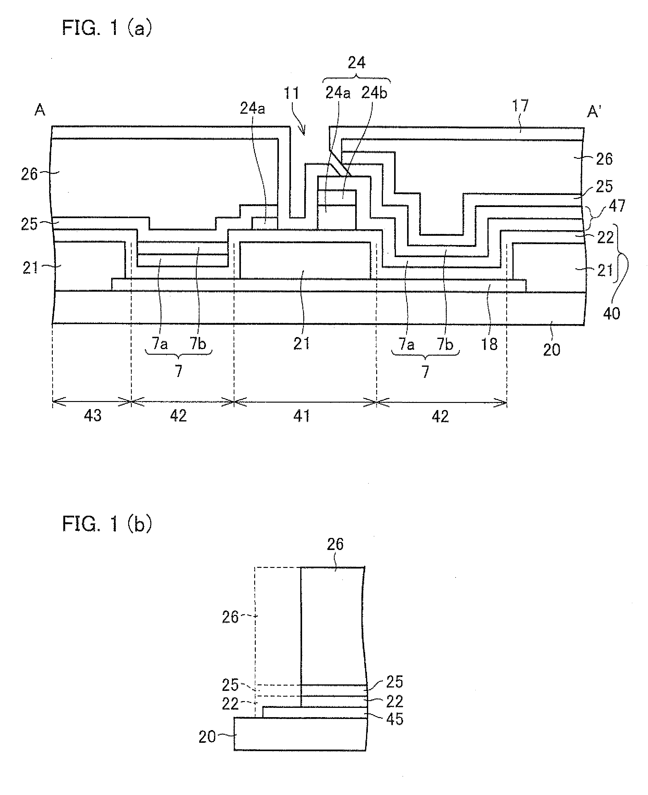
[0073]A first embodiment of the present invention is described below with reference to FIGS. 1 through 5.
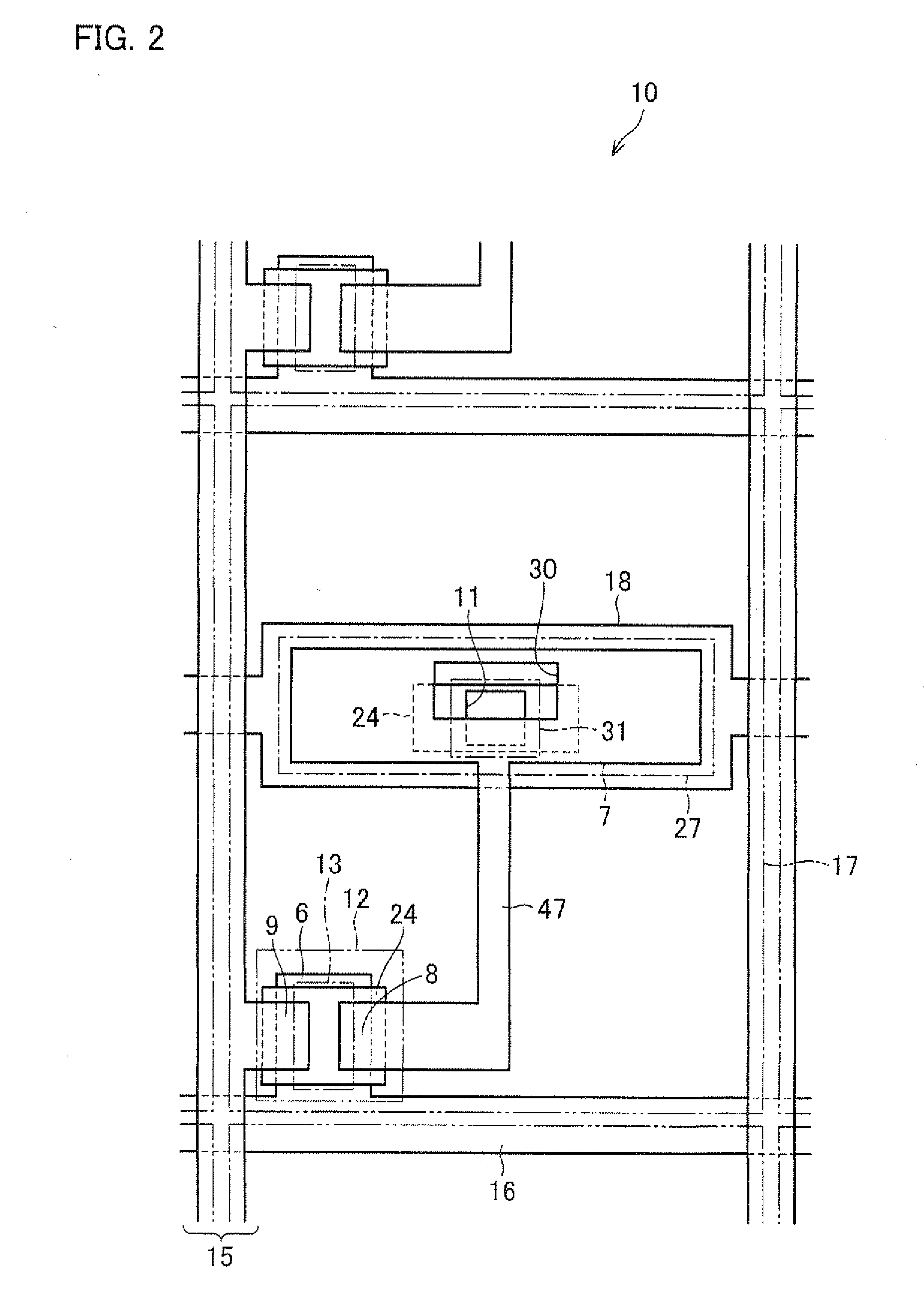
[0074]FIG. 2 is a plan view schematically illustrating an arrangement of an active matrix substrate 10 in accordance with the present embodiment, and FIG. 3 is an enlarged view illustrating the vicinity of a storage capacitor wire of the active matrix substrate illustrated in FIG. 1, and FIG. 1 is a cross-sectional view taken along the line A-A′ in FIG. 3.
[0075]The active matrix substrate 10 includes, as illustrated in FIG. 2, a scanning signal line 16 formed in a horizontal direction in FIG. 2, a data signal line 15 formed in a perpendicular direction in FIG. 2, both of which are formed so as to orthogonalize each other, a TFT 12 (Thin Film Transistor) formed in the vicinity of each intersection of these two lines (15 and 16), and a pixel electrode 17. The TFT 12 includes a source electrode 9 which is connected with the data signal line 15, and a drain electrode 8 which is conne...
second embodiment
[0123]The following description deals with the second embodiment of the present invention with reference to FIGS. 6(a), 6(b) and 7.
[0124]FIG. 6(a) is an enlarged view illustrating the vicinity of the storage capacitor wire of the active matrix substrate in accordance with the present embodiment, and FIG. 7 is a cross-sectional view taken along the line B-B′ in FIG. 6(a).
[0125]In the active matrix substrate according to the present invention, as will be described below, a storage capacitor wire 218 and the gate insulating film (not illustrated) having a multi-layer structure (a first gate insulating layer and a second gate insulating layer) is formed on a substrate, and thereon, a drain electrode (with a drain lead-out wire 247 and a drain lead-out electrode 207), an interlayer insulating film (not illustrated), and a pixel electrode 217 are formed in this order. The drain lead-out electrode 207 is formed so as to be located on the storage capacitor wire 218.
[0126]As illustrated in F...
third embodiment
[0139]The following description deals with the third embodiment of the present invention with reference to FIGS. 9, 10(a) and 10(b).
[0140]FIG. 9 is an enlarged view illustrating the vicinity of a storage capacitor wire of an active matrix substrate in accordance with the present invention, and FIG. 10(a) is a cross-sectional view taken along line C-C′ illustrated in FIG. 9.
[0141]In the active matrix substrate according to the present invention, as will be described below, a storage capacitor wire 318 and a gate insulating film (not illustrated) having a multi-layer structure (a first gate insulating layer and a second gate insulating layer) are formed, and thereon, a drain electrode (with a drain lead-out electrode wire 347 and a drain lead-out electrode 307), an interlayer insulating film (not illustrated), and a pixel electrode 317 are formed in this order. The drain lead-out electrode 307 is formed so as to be on the storage capacitor wire 318.
[0142]As illustrated in FIG. 9, an a...
PUM
| Property | Measurement | Unit |
|---|---|---|
| diameter | aaaaa | aaaaa |
| width | aaaaa | aaaaa |
| width | aaaaa | aaaaa |
Abstract
Description
Claims
Application Information