Substrate for mounting an optical semiconductor element, manufacturing method thereof, an optical semiconductor device, and manufacturing method thereof

a technology of optical semiconductor elements and substrates, which is applied in semiconductor devices, solid-state devices, printed circuit manufacturing, etc., can solve the problems of reduced brightness, increased temperature of optical semiconductor elements, and high thermal resistance, so as to enhance the reliability of optical semiconductor devices, reduce the effect of thermal resistance and reduced thermal resistan

Active Publication Date: 2009-04-16
RESONAC CORP
View PDF1 Cites 30 Cited by
  • Summary
  • Abstract
  • Description
  • Claims
  • Application Information

AI Technical Summary

Benefits of technology

[0030]According to the substrate for mounting optical semiconductor element of this invention, heat dissipated from the optical semiconductor element mounted on the substrate surface is transported to the mounting substrate via the heat conduction path of an external connection terminal on the substrate rear portion, positioned directly below the optical semiconductor element. As a result, increases in temperature of the optical semiconductor element and optical semiconductor device are suppressed, and the reliability of the optical semiconductor device can be enhanced. Moreover, according to a method for manufacturing the optical semiconductor element mounting substrate and a method of for manufacturing an optical semiconductor device of this invention, manufacturing processes in such method can be simplified, so that productivity can be enhanced and costs can be lowered.

Problems solved by technology

Hence because the distance from the light-emitting element which is the heat source to the external electrodes is long, thermal resistance is high, and due to this structure, increases in the temperature of the optical semiconductor element are unavoidable.
Increases in the temperature of the optical semiconductor element cause degradation of the optical semiconductor element, and induce reduced brightness, shortened lifetimes, and other declines in the performance and reliability of the optical semiconductor device, and so are undesirable.
However, when a heat sink or metal / ceramic package with high thermal conductivity or similar are used as members employing materials with high thermal conductivity, the overall number of components as well as the number of manufacturing processes are increased, which tend to increase costs and detract from manufacturing productivity.
However, when this board is formed as a large molded object of size 20 mm2 or larger, in which are arranged a plurality of optical semiconductor elements in a matrix as shown in FIG. 2A and FIG. 2B, differences in linear expansion rates give rise to stress-induced warping, and it becomes difficult to execute subsequent processes, among other problems.
Further, there is a tendency for resin to be not sufficiently filled between circuit wires in circuits in which optical semiconductor elements and external connection elements are arranged in a complex manner for electric input.
If resin is not sufficiently filled between circuit wires and thereby unfilled portions of resin exist, when subsequently filling the depressed portion with transparent sealing resin, transparent resin may leak from the unfilled portions, so that filling faults may occur, and execution of subsequent manufacturing processes becomes difficult.

Method used


Image

  • Substrate for mounting an optical semiconductor element, manufacturing method thereof, an optical semiconductor device, and manufacturing method thereof
  • Substrate for mounting an optical semiconductor element, manufacturing method thereof, an optical semiconductor device, and manufacturing method thereof
  • Substrate for mounting an optical semiconductor element, manufacturing method thereof, an optical semiconductor device, and manufacturing method thereof

Examples


example 1

(a) Base Substrate Processing

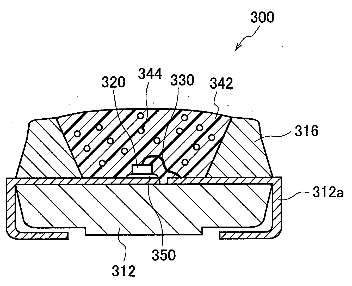
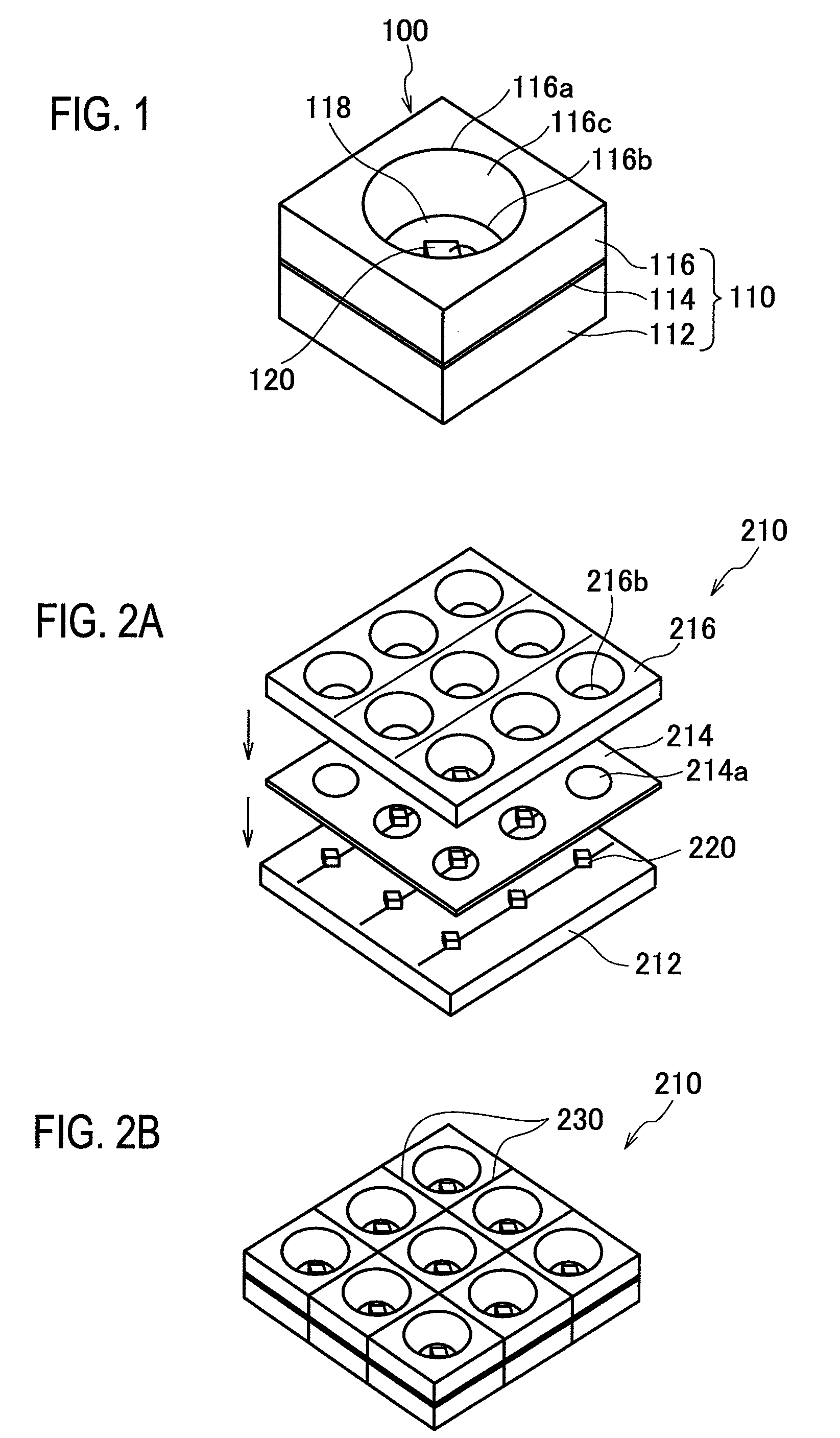
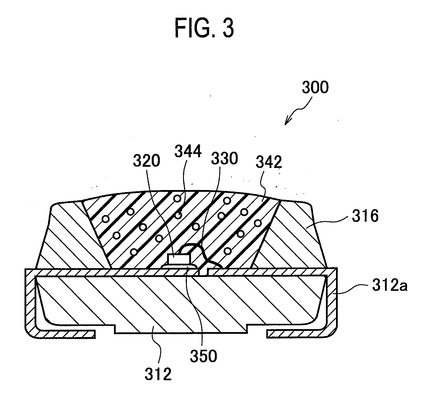
[0089]A laminated board, MCL-E-679F (product name, manufactured by Hitachi Chemical Co., Ltd.), with he base substrate of overall thickness 0.1 mm, and copper foil on the upper face of thickness 18 μm, was used; by irradiating the lower face (insulating layer) side with a carbon dioxide gas laser, holes of diameter 1 mm were opened, the insulating layer was penetrated to reach the copper foil, and in this way ten non-penetrating holes (openings for external connection terminal formation) were formed. The processing to open holes was performed at positions directly below positions for mounting of optical semiconductor elements.

[0090]Next, a well-known subtraction method was used to pattern the copper foil, to form wiring circuits. And, by applying a white solder resist onto the wiring circuits thus formed, a board with wiring circuits, having a wiring circuit protection resist layer, was fabricated. The layer structure of the board is shown in FIG. 7A.

[00...

example 2

[0094]Except for using, as the base substrate, a flexible substrate comprising copper foil and a polyimide film as the insulating layer, a method entirely similar to Example 1 was used to fabricate a substrate for mounting optical semiconductor element.

example 3

[0095]Except for using a base substrate onto which a lead frame and organic insulating layer had been bonded applying heat and pressure, a method entirely similar to Example 1 was used to fabricate a substrate for mounting optical semiconductor element.


PUM


Abstract

A substrate for mounting optical semiconductor elements is provided, including a base substrate having an insulating layer and a plurality of wiring circuits formed on the upper face of the insulating layer, and having at least one external connection terminal formation opening portion which penetrates the insulating layer and reaches the wiring circuits; and an optical reflection member, which is provided on the upper face of the base substrate, and which forms at least one depressed portion serving as an area for mounting an optical semiconductor element.

Description

BACKGROUND OF THE INVENTION[0001]1. Field of the Invention[0002]The present invention relates to a substrate for mounting an optical semiconductor element, a manufacturing method thereof, an optical semiconductor device using such a substrate, and a method of manufacturing an optical semiconductor device.[0003]2. Description of the Related Art[0004]In recent years, in addition to reductions in size and weight, there have been advances in the performance and multifunctionality in the field of electronic equipment, and electronic components have come to be mounted at high densities in electronic equipment. What are called SMDs (Surface Mount Devices), which can be mounted on the surface of print boards, have come to be the mainstream of electronic components used in electronic equipment; SMDs can be connected to wiring patterns on print boards by reflow soldering and other methods, and are used in various applications.[0005]For example, SMD type LEDs (Light-Emitting Diodes) are electr...

Claims


Application Information

Patent Timeline
Patent Type & Authority Applications(United States)
IPC IPC(8): H01L33/00H01L33/48
CPCH01L25/0753H01L2224/97H05K3/3436H01L24/97H01L2224/48091H01L2224/48247H01L2224/73265H01L33/486H01L2924/12041H01L2224/32245H01L2224/45144H01L2924/00014H01L2924/00H01L2224/85H01L2924/12042H01L2924/181H01L2924/00012
Inventor KOTANI, HAYATOURASAKI, NAOYUKIMIZUTANI, MAKOTO
Owner RESONAC CORP
Why Eureka
Try Eureka