Semiconductor light emitting device

a technology of semiconductor layer and light source, which is applied in the direction of semiconductor devices, lasers, semiconductor lasers, etc., can solve the problems of difficult to achieve excellent ohmic contact with the nonpolar plane of the gan semiconductor layer

Active Publication Date: 2009-04-16
ROHM CO LTD
View PDF12 Cites 91 Cited by
  • Summary
  • Abstract
  • Description
  • Claims
  • Application Information

AI Technical Summary

Benefits of technology

[0010]An object of the present invention is to provide a semiconductor light emitting device that has an excellent ohmic contact of n-

Problems solved by technology

In other words, it is difficult to attain excellent ohmic contact with the nonpolar plane of the GaN semiconductor layer.
Needless to say, a similar problem arises not only

Method used


Image

  • Semiconductor light emitting device
  • Semiconductor light emitting device
  • Semiconductor light emitting device

Examples


Embodiment Construction

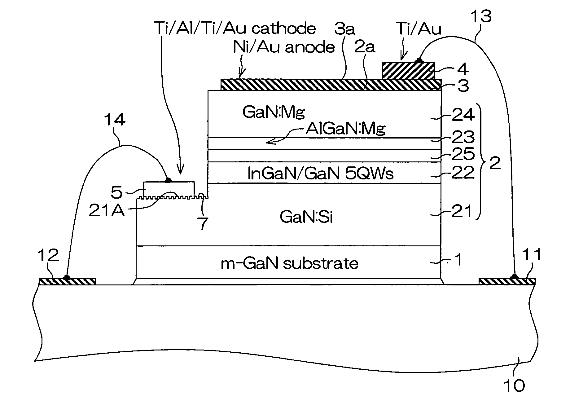
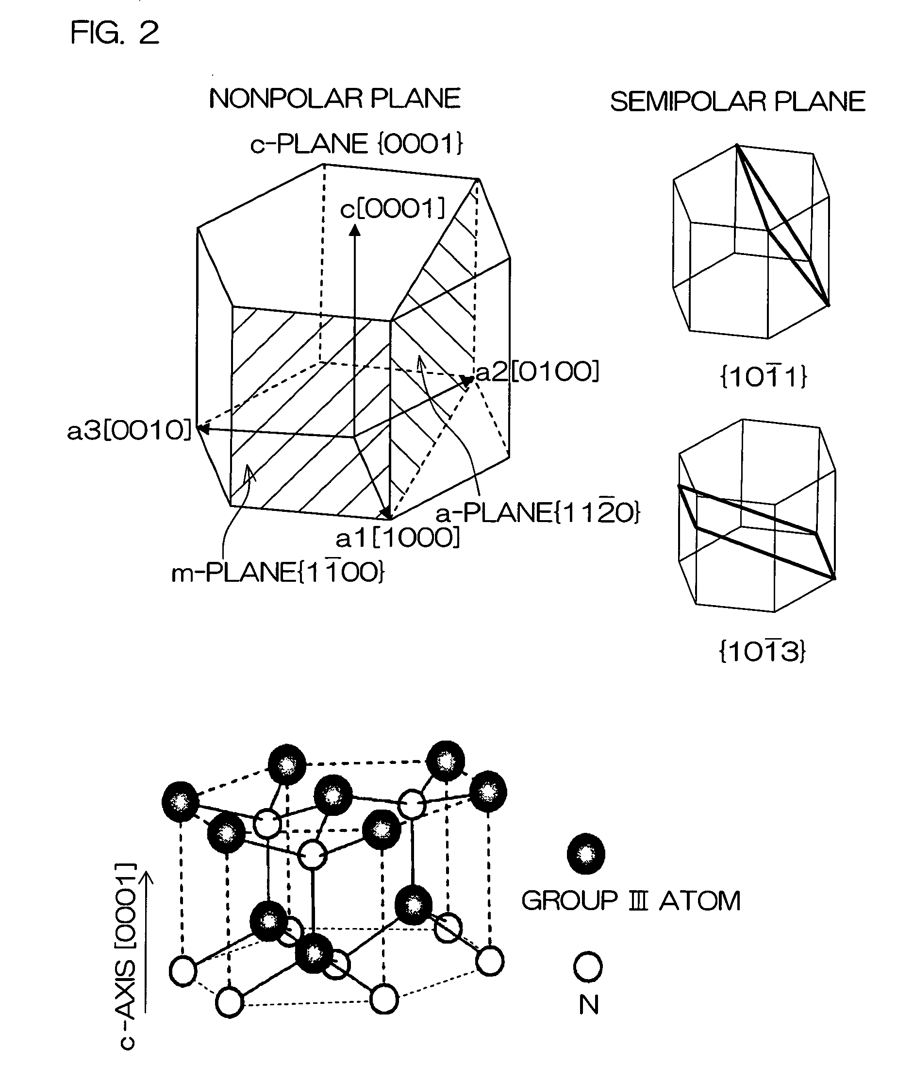
[0024]A semiconductor light emitting device according to an embodiment of the present invention has a device body made of a group III nitride semiconductor having a major surface defined by a nonpolar plane, and a contact portion of the device body with an n-type electrode includes a crystal plane (a polar plane or a semipolar plane) different from the major surface.

[0025]According to this structure, the contact portion of the device body, made of the group III nitride semiconductor having the major surface defined by the nonpolar plane, with the n-type electrode includes the crystal plane different from the major surface, i.e., a polar plane or a semipolar plane. The polar or semipolar plane forms excellent ohmic contact with the n-type electrode. Therefore, the n-type electrode can excellently come into ohmic contact with the contact portion of the device body.

[0026]The contact portion may have only a nonpolar plane, only a semipolar plane, both of a nonpolar plane and a semipolar...


PUM


Abstract

A semiconductor light emitting device has a device body made of a group III nitride semiconductor having a major surface defined by a nonpolar plane. In the device body, a contact portion with an n-type electrode includes a crystal plane different from the major surface. For example, the contact portion may include a corrugated surface. More specifically, the contact portion may include a region having a plurality of protrusions parallel to a polar plane formed in a striped manner.

Description

BACKGROUND OF THE INVENTION[0001]1. Field of the Invention[0002]The present invention relates to a semiconductor light emitting device (such as a light emitting diode or a laser diode) employing a group III nitride semiconductor.[0003]2. Description of Related Art[0004]Group III nitride semiconductors are group III-V semiconductors employing nitrogen as a group V element, and typical examples thereof include aluminum nitride (AlN), gallium nitride (GaN) and indium nitride (InN), which can be generally expressed as AlxInyGa1-x-yN (0≦x≦1, 0≦y≦1 and 0≦x+y≦1).[0005]A method of manufacturing a nitride semiconductor by growing a group III nitride semiconductor on a gallium nitride (GaN) substrate having a major surface defined by a c-plane by metal organic chemical vapor deposition (MOCVD) is known in general. This method is so applied that a GaN semiconductor multilayer structure having an n-type layer and a p-type layer can be formed, and a light emitting device can be prepared using su...

Claims


Application Information

Patent Timeline
IPC IPC(8): H01L33/00H01L33/06H01L33/32H01L33/40
CPCB82Y20/00H01L33/16H01L33/22H01L33/32H01L33/38H01S5/34333H01L33/40H01S5/0425H01S5/2009H01S5/22H01S5/3202H01L33/382H01S5/0283H01S5/0287H01S5/2201H01S5/04254H01S5/32025
Inventor TANAKA, TAKETOSHIOKAMOTO, KUNIYOSHI
Owner ROHM CO LTD
Why Eureka
Try Eureka