
Display Device and Method for Manufacturing Display Device

a technology of display device and display tube, which is applied in the direction of discharge tube/lamp details, discharge tube luminescnet screen, discharge tube/lamp details, etc., can solve the problems of long time required for inorganic film formation and etching process, large expensive vacuum apparatus, and inability to meet the needs of use, etc., to achieve low cost, reduce the effect of vacuum apparatus and high material use efficiency

Inactive Publication Date: 2009-04-16
SEMICON ENERGY LAB CO LTD
View PDF24 Cites 33 Cited by
  • Summary
  • Abstract
  • Description
  • Claims
  • Application Information

AI Technical Summary

Benefits of technology

[0008]It is another object of the present invention to provide a display device with high image quality and reliability or a large-sized display device with a large screen at low cost with high productivity.
[0039]Since expensive facilities such as a large vacuum apparatus can be reduced and a function layer having functionality which is used for a display element can be manufactured by a wet process, material use efficiency is higher, and reduction in cost and high productivity can be achieved. Thus, according to the present invention, highly reliable display devices and electronic devices can be manufactured at low cost with improved productivity.

Problems solved by technology

However, in order to perform liquid repellent treatment by the above method, a large expensive vacuum apparatus is necessary.
However, in the case where a thin film with a thickness of several micrometers, such as a color filter is formed, there is a problem in that a long time is needed for formation of an inorganic film and an etching process, which is not practical.

Method used


Image

  • Display Device and Method for Manufacturing Display Device
  • Display Device and Method for Manufacturing Display Device
  • Display Device and Method for Manufacturing Display Device

Examples


embodiment mode 1

[0064]This embodiment mode will describe an example of a function layer in a display device aimed at higher image quality and higher reliability, which can be manufactured at low cost with high productivity.

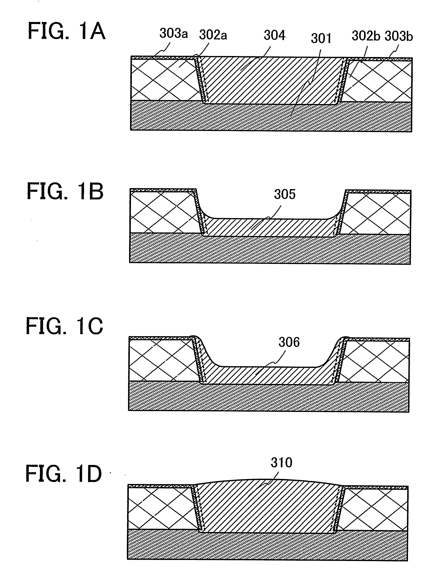
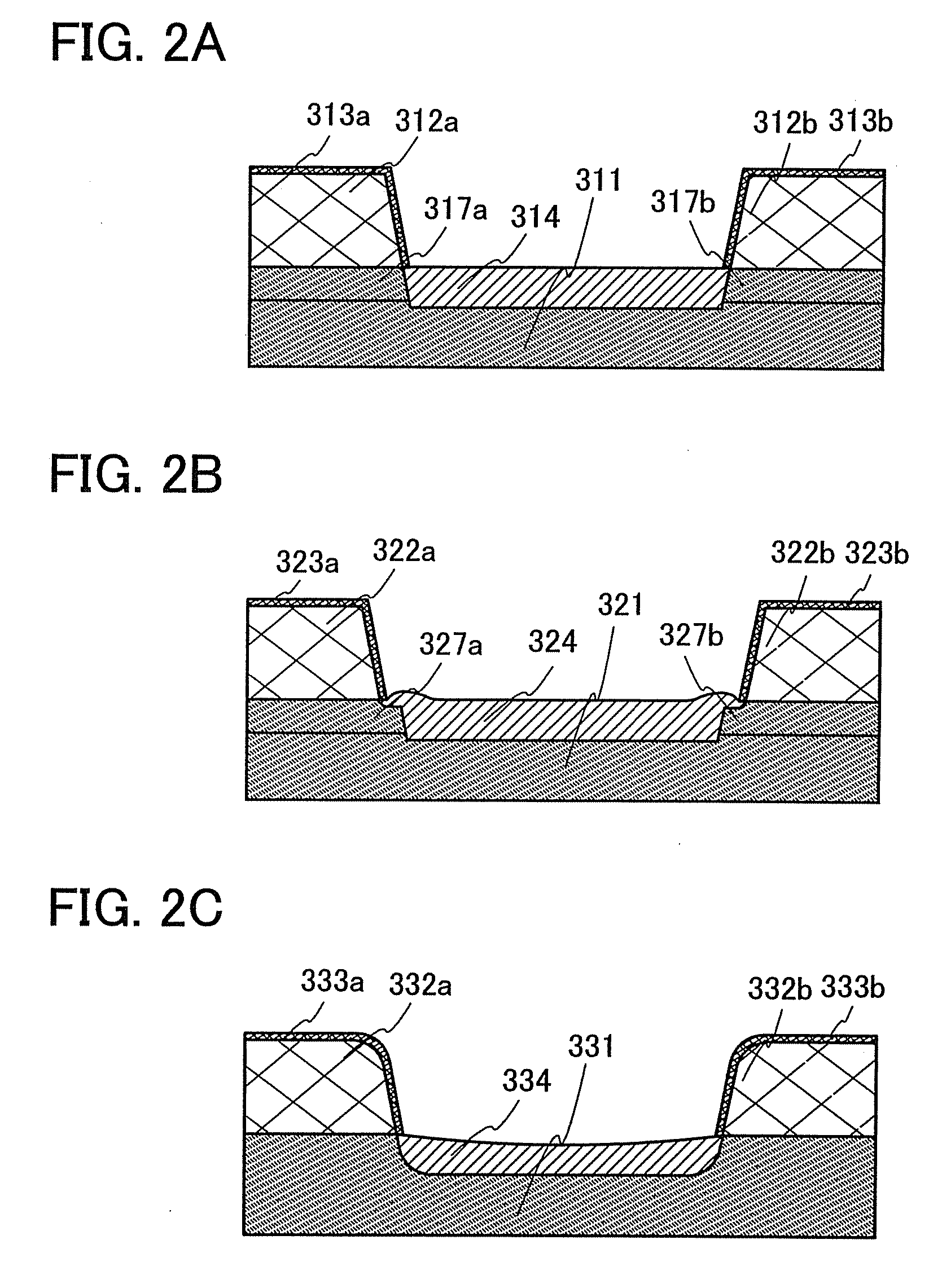
[0065]FIGS. 1A to 1D and FIGS. 2A to 2C show an example of a function layer of the present invention. FIG. 1A shows an example in which in an opening formed with a layer 301 including an organic compound (a first organic compound) and layers 302a and 302b including an organic compound (a second organic compound), a function layer 304 is formed so that the opening can be filled with the function layer 304. Oxide layers 303a and 303b are formed on surfaces of the layers 302a and 302b including an organic compound to be interposed between the function layer 304 and the layers 302a and 302b. The layer 301 including an organic compound at a base of the opening is a region with the small thickness and a depressed portion is formed because an oxide layer formed on a surface of the layer...

embodiment mode 2

[0113]This embodiment mode will describe an example of a display device aimed at higher image quality and higher reliability, which can be manufactured at low cost with high productivity. More specifically, a passive matrix display device is shown.

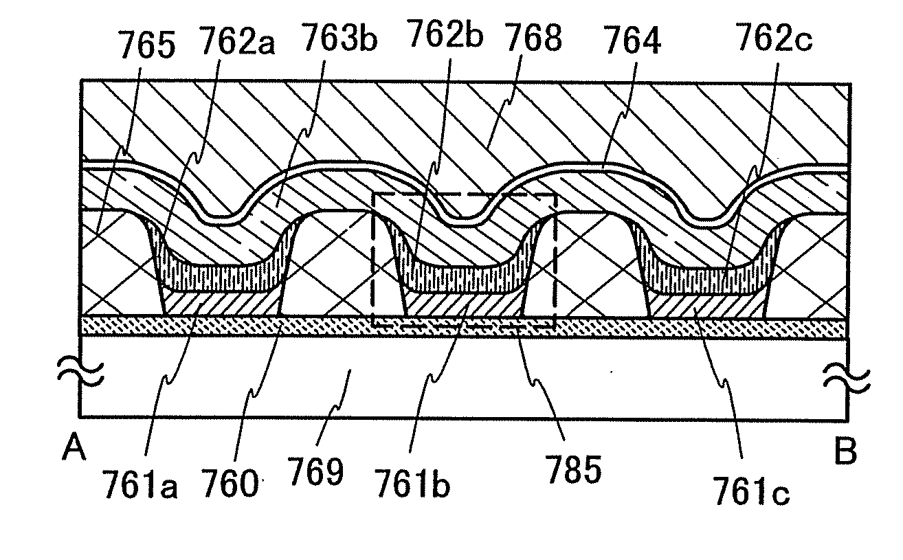
[0114]FIGS. 4A and 4B each show a passive matrix liquid crystal display device to which the present invention is applied. FIG. 4A illustrates a reflective liquid crystal display device and FIG. 4B illustrates a transmissive liquid crystal display device. In FIGS. 4A and 4B, a substrate 1700 and a substrate 1710 are provided opposite to each other with a liquid crystal layer 1703 interposed therebetween. The substrate 1700 is provided with electrode layers 1701a, 1701b, and 1701c also referred to as pixel electrode layers, which are used for display elements 1713 and an insulating layer 1712 serving as an alignment film, coloring layers 1706a, 1706b, and 1706c serving as part of a color filter, a layer 1720 including an organic compound, a ...

embodiment mode 3

[0155]This embodiment mode will describe an example of a display device aimed at higher image quality and higher reliability, which can be manufactured at low cost with high productivity. Specifically, this embodiment mode illustrates a liquid crystal display device that uses liquid crystal elements as display elements. Note that, this embodiment mode describes an active matrix liquid crystal display device, which is different from Embodiment Mode 2.

[0156]FIG. 8A is a top view of a liquid crystal display device which is one mode of the present invention. FIG. 8B is a cross-sectional view taken along a line C-D in FIG. 8A.

[0157]As shown in FIG. 8A, a pixel region 606 and driver circuit regions 608a and 608b which are scan line driver circuits are sealed between a substrate 600 and a counter substrate 695 with a sealing material 692. In addition, a driver circuit region 607 which is a signal line driver circuit including a driver IC is provided over the substrate 600. In the pixel reg...


PUM

PropertyMeasurementUnit
Thicknessaaaaaaaaaa
Electrical conductoraaaaaaaaaa

Abstract

To provide a display device with higher image quality and reliability or a large-sized display device with a large screen at low cost with high productivity. A function layer (such as a coloring layer or a pixel electrode layer) used in the display device is formed by discharging a liquid function-layer-forming material to an opening formed with a layer including a first organic compound which has a C—N bond or a C—O bond in the main chain as a base and a layer including a second organic compound as a partition. The fluorine density exhibiting liquid repellency to the liquid function-layer-forming material, which is attached to a surface of the layers including organic compounds, is controlled, whereby a liquid repellent region and a lyophilic region can be selectively formed.

Description

BACKGROUND OF THE INVENTION[0001]1. Field of the Invention[0002]The present invention relates to a display device which has a display element and a method for manufacturing the display device.[0003]2. Description of the Related Art[0004]When a function layer such as a color filter used in a display device is formed by an inkjet method, a liquid repellent region and a lyophilic region, where modification treatment is performed with respect to a thin-film material liquid are used in a region where a thin film is to be formed in order to make the thin film have a high definite micropattern.[0005]For example, a bank which is a partition member of the thin film has a stacked structure of a bank formed of an inorganic material and a bank formed of an organic material, and only a surface of the bank formed of an organic material is made to have liquid repellency by plasma treatment using a fluorine-based gas, whereby a liquid repellent region and a lyophilic region with respect to the thin...

Claims


Application Information

Patent Timeline
IPC IPC(8): H01J1/63H01L51/56
CPCH01L27/3246H01L51/0004H01L27/3283H10K59/122H10K59/173H10K71/13
Inventor FUJII, GENTAKAHASHI, ERIKAKIKUCHI, ERUMUKAWAKAMI, SACHIKO
Owner SEMICON ENERGY LAB CO LTD
Learn More