Ferromagnetic tunnel junction element, magnetic recording device and magnetic memory device

Inactive Publication Date: 2009-04-16
FUJITSU LTD
View PDF4 Cites 28 Cited by
  • Summary
  • Abstract
  • Description
  • Claims
  • Application Information

AI Technical Summary

Benefits of technology

[0010]In accordance with an aspect of an embodiment, a ferromagnetic tunnel junction element includes a pinned layer wherein at least a part of a magnetization direction is held, an insulation layer formed on the pinned layer, creating an energy barrier that electrons can flow through by a tunnel effect, and a first free layer formed on the insulation layer made of a first ferromagnetic material containing boron atoms. T

Problems solved by technology

There is a known problem that such a ferromagnetic tunnel junction element shows a high MR ratio, 200% and greater, at ambient temperatures.
However, where the free layer of the ferromagnetic tunnel junction element is constructed into a single-layered structure, the coercivity tends to be greater, which makes the soft magnetic property inferior.
This brings a problem such that—if applying the weak external magnetic field,

Method used


Image

  • Ferromagnetic tunnel junction element, magnetic recording device and magnetic memory device
  • Ferromagnetic tunnel junction element, magnetic recording device and magnetic memory device
  • Ferromagnetic tunnel junction element, magnetic recording device and magnetic memory device

Examples


example 1

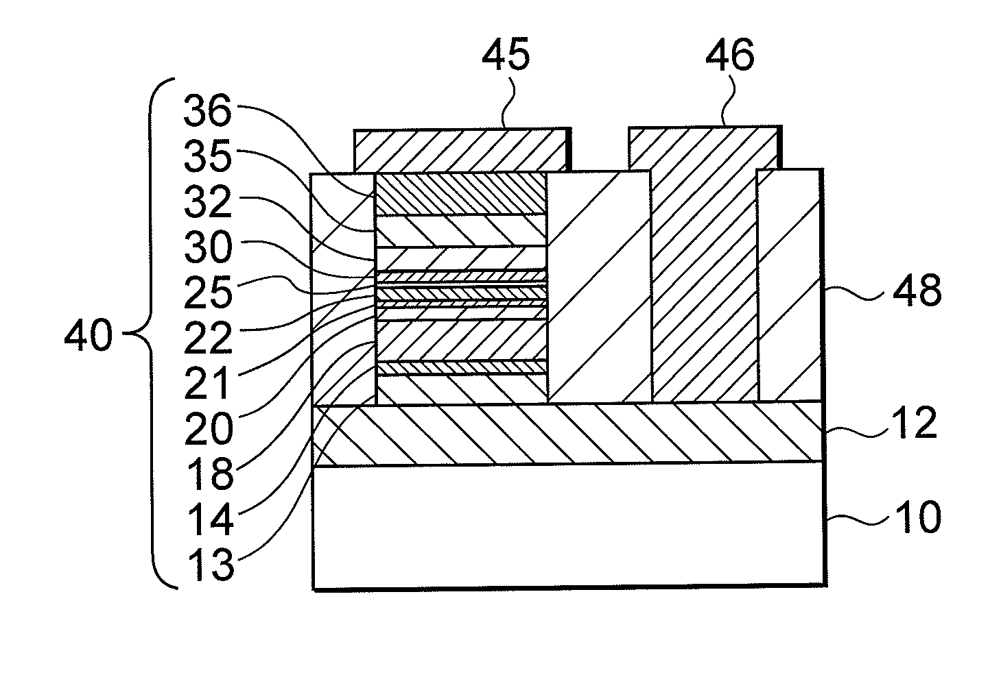
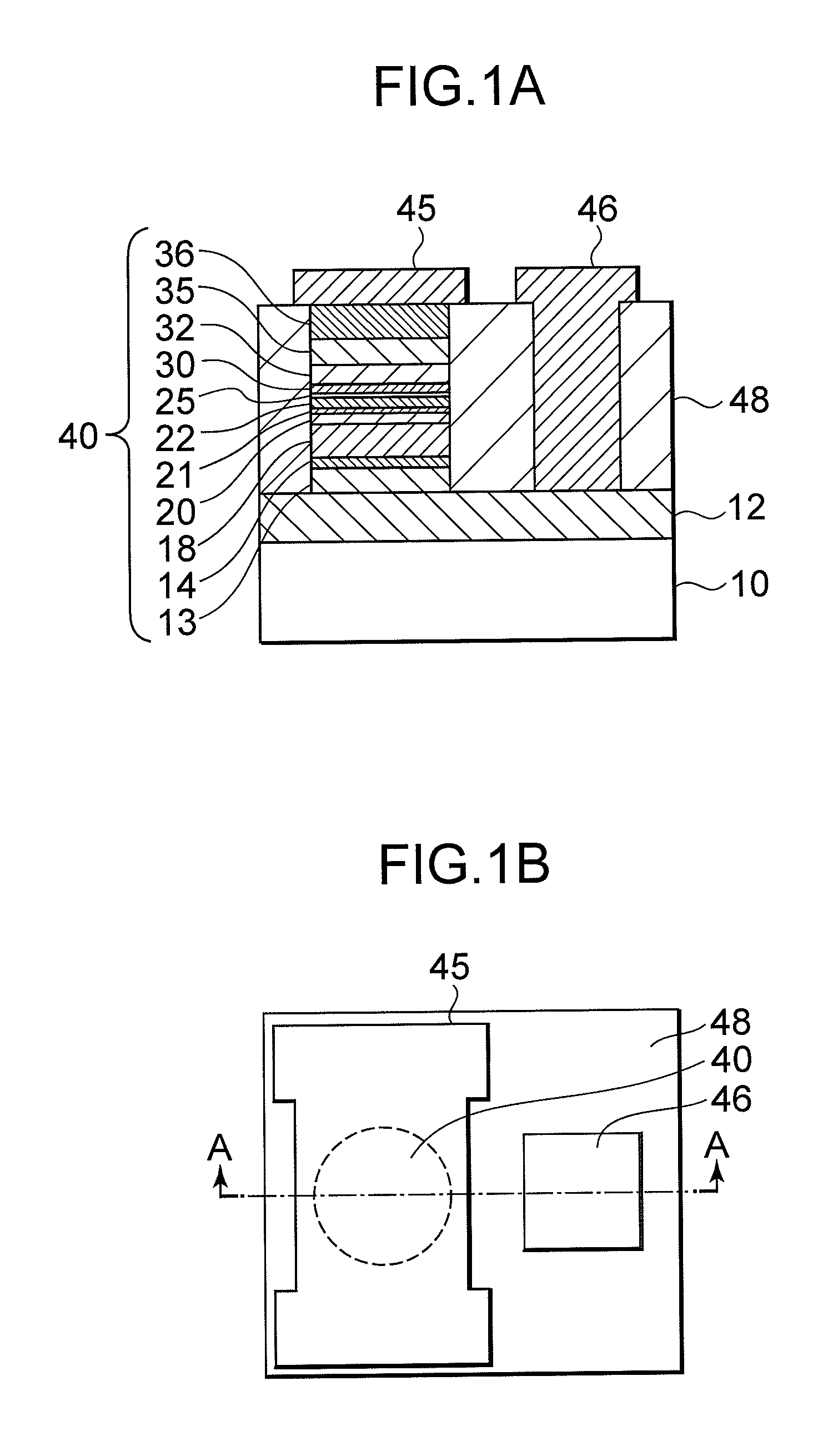
[0089]The element in the first example having the same structure of the ferromagnetic tunnel junction element shown in FIG. 1 is produced by the following manner.

[0090]Using a magnetron sputter device, the layered body shown in FIG. 3A is formed in the following manner: 1). The conductive layer 12 made of NiFe is formed on the Si substrate 10 covered with the SiO2 layer. 2). The surface of the layered body is leveled by chemical mechanical polishing (CMP). 3). The surface of the conductive layer 12 is cleansed by Ar reverse sputtering. 4). A 5 nm thickness of the first underlayer 13 made of Ta is formed on the conductive layer 12. Then, 5). A 2 nm thickness of the second underlayer 14 made of Re is formed, followed by 6). A 7 nm thickness of the pinning layer 18 made of Ir21Mn79, 7). A 2 nm thickness of the first pinned layer 20 made of Co74Fe26.8). 8). A 0.8 nm thickness of the nonmagnetic junction layer 21 made of Ru, 9). A 2 nm thickness of the second pinned layer 22 made of CO60...

example 2

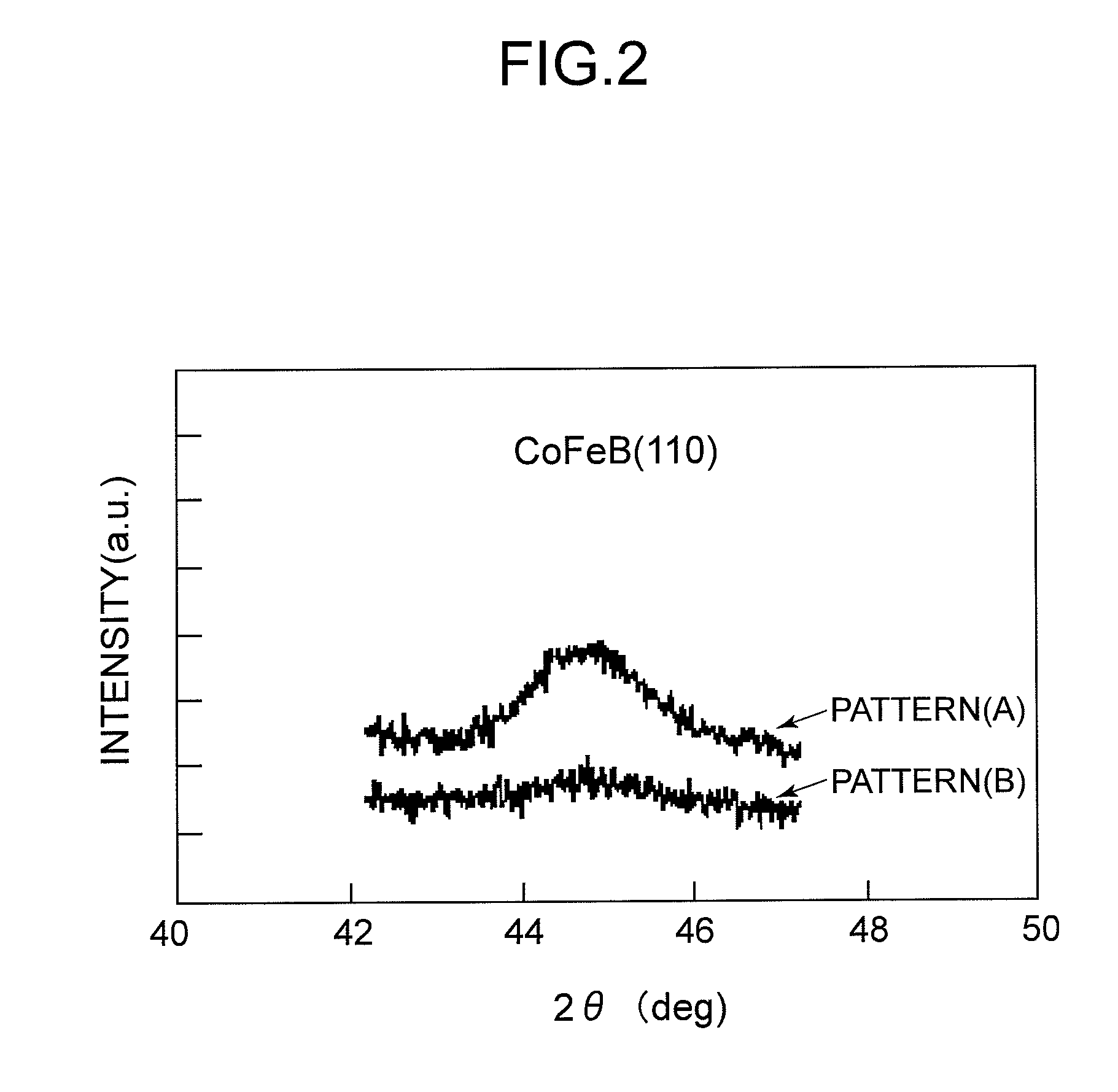
[0092]The ferromagnetic tunnel junction element in the second example is formed in the same manner of the first example except: making the first free layer 30 (2 nm) of Co71Fe24B5 instead of Co60Fe20B20, and making the second free layer 32 (4 nm) of Ni85.5Fe9.5B5 instead of Ni72Fe8B20.

example 3

[0093]The ferromagnetic tunnel junction element in the third example is formed in the same manner of the first example except: making the first free layer 30 (2 nm) of Co67.5Fe22.5B10 instead of CO60Fe20B20, and making the second free layer 32 (4 nm) of Ni81Fe9B10 instead of Ni72Fe8B20.


PUM


Abstract

A ferromagnetic tunnel junction element is a magnetoresistance effect element wherein an electric resistance varies in accordance with a magnetic field applied. The ferromagnetic tunnel junction element includes a pinned layer wherein at least a part of a magnetization direction is held, and an insulation layer formed on the pinned layer, creating an energy barrier that electrons can flow through by a tunnel effect. A first free layer made of a first ferromagnetic material containing boron atoms, is formed on the insulation layer. In the first free layer, a direction of the magnetization switches under an influence of an external magnetic field. A second free layer made of a first ferromagnetic material containing boron atoms, is formed on the first free layer. The direction of magnetization of the second free layer switches under the influence of the external magnetic field, exchanging and coupling with the first free layer.

Description

BACKGROUND OF THE INVENTION[0001]1. Field of the Invention[0002]This invention relates to a ferromagnetic tunnel junction element that is a magnetoresistance effect element wherein an electric resistance varies in accordance with a magnetic field applied.[0003]2. Description of the Related Art[0004]A ferromagnetic tunnel junction element has a ferromagnetic metal / insulation layer / ferromagnetic metal-structure and an insulation layer thereof that produces an energy barrier that electrons can penetrate by the tunnel effect. In this specification, “ / ” means “and”. For the ferromagnetic tunnel junction element, a tunnel probability (tunnel resistance) depends on magnetization states of upper and lower magnetic layers. This means that the tunnel resistance can be controlled by controlling the magnetization states of the ferromagnetic metals by applying an external magnetic field. Typically, the ferromagnetic tunnel junction element has a pinned layer / insulation layer / free layer-structure...

Claims


Application Information

Patent Timeline
IPC IPC(8): G11B5/33
CPCB82Y10/00B82Y25/00G11B5/3906G11B5/3909G11C11/16H01F10/3295H01F10/3254H01F10/3272H01L27/228H01L43/10H01F10/3204G11C11/1659G11C11/161G11C11/1657H10B61/22H10N50/85G11B5/39G11C11/15H10N50/10H10N50/01
Inventor SATO, MASASHIGEUMEHARA, SHINJIROIBUSUKI, TAKAHIRO
Owner FUJITSU LTD
Why Eureka
Try Eureka