Boron-doped nanocrystalline diamond film and preparation method thereof

A nano-diamond, boron-doped technology, applied in metal material coating process, coating, gaseous chemical plating and other directions, can solve the problems of poor p-type conductivity and electrochemical performance, and achieve improved conductivity and good conductivity. ability, the effect of improving electrochemical performance

Inactive Publication Date: 2011-01-26
ZHEJIANG UNIV OF TECH
View PDF2 Cites 16 Cited by
  • Summary
  • Abstract
  • Description
  • Claims
  • Application Information

AI Technical Summary

Problems solved by technology

[0004] Aiming at the problem that the p-type conductivity and electrochemical performance of the boron-doped nano-diamond film are worse than those of the microcrystalline diamond film doped with the same concentration

Method used


Image

  • Boron-doped nanocrystalline diamond film and preparation method thereof
  • Boron-doped nanocrystalline diamond film and preparation method thereof
  • Boron-doped nanocrystalline diamond film and preparation method thereof

Examples


Embodiment 1

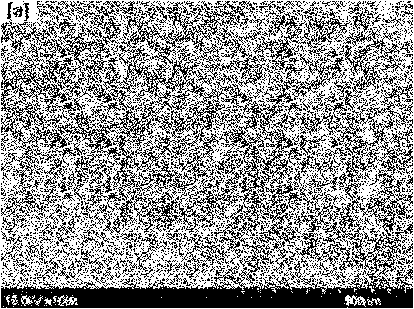
[0030] Polish the monocrystalline silicon wafer with nano-scale diamond powder, and the grinding time is about half an hour. After the polished silicon wafer is cleaned by an ultrasonic machine, it is used as the substrate for the growth of the nano-diamond film. Using hot wire chemical vapor deposition method (chemical vapor deposition equipment purchased from Shanghai Jiaoyou Diamond Coating Co., Ltd.), using acetone as carbon source, B 2 h 6 as the boron source, the boron concentration is 500 ppm; acetone is brought into the reaction chamber by hydrogen bubbling, the temperature of the reaction chamber is controlled at 600~700°C, the preparation time is 5 hours, and the boron doped with a thickness of 12.1 μm is prepared nanodiamond film.

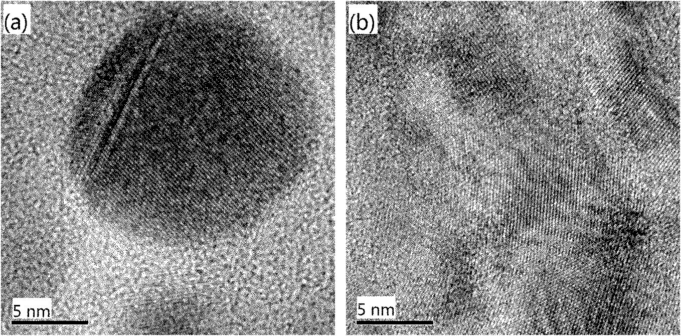
[0031] Place the prepared thin film in a quartz tube, use a vacuum pump to pump out the air in the quartz tube, the relative vacuum degree is 5torr (1 torr is 1 millimeter of mercury column (mmHg)), then seal the quartz tube, and annea...

Embodiment 2

[0036] The monocrystalline silicon wafer is polished with nanometer diamond powder, and the polishing time is about half an hour. After the polished silicon wafer is cleaned by an ultrasonic machine, it is used as the substrate for the growth of the nano-diamond film. Using hot wire chemical vapor deposition method (chemical vapor deposition equipment purchased from Shanghai Jiaoyou Diamond Coating Co., Ltd.), using acetone as carbon source, B 2 h 6 As a boron source, the boron concentration is 500 ppm; acetone is brought into the reaction chamber by hydrogen bubbling, the temperature of the reaction chamber is controlled at 600-700°C, the preparation time is 6 hours, and a nano-diamond film with a thickness of 12.1 μm is prepared .

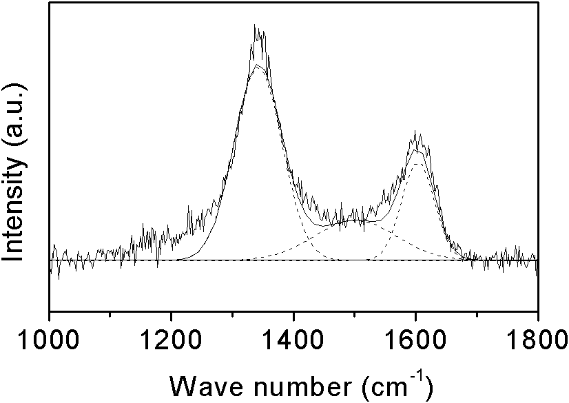
[0037] The prepared film was placed in a quartz tube, and the air in the quartz tube was pumped out with a vacuum pump to a relative vacuum of 5 torr, and then the quartz tube was sealed and annealed in vacuum at 1150° C. for 30 minutes. Raman...

Embodiment 3

[0041] The monocrystalline silicon wafer is polished with nanometer diamond powder, and the polishing time is about half an hour. After the polished silicon wafer is cleaned by an ultrasonic machine, it is used as the substrate for the growth of the nano-diamond film. Using hot wire chemical vapor deposition method (chemical vapor deposition equipment purchased from Shanghai Jiaoyou Diamond Coating Co., Ltd.), using acetone as carbon source, B 2 h 6 As a boron source, the boron concentration is 5000 ppm; acetone is brought into the reaction chamber by hydrogen bubbling, the temperature of the reaction chamber is controlled at 600-700°C, the preparation time is 6 hours, and a nano-diamond film with a thickness of 12.3 μm is prepared .

[0042] The prepared film was placed in a quartz tube, and the air in the quartz tube was pumped out with a vacuum pump to a relative vacuum of 5 torr, and then the quartz tube was sealed and annealed in vacuum at 1000° C. for 60 minutes. Adop...


PUM

PropertyMeasurementUnit
Diameteraaaaaaaaaa
Oxygen evolution potentialaaaaaaaaaa
Current densityaaaaaaaaaa

Abstract

The invention provides a boron-doped nanocrystalline diamond film. The boron-doped nanocrystalline diamond film is prepared by using the following steps of: preparing a boron-doped nanocrystalline diamond film on a monocrystalline silicon substrate by adopting a CVD (Chemical Vapor Deposition) method and annealing the film in vacuum at 800-1200 DEG C for 30-60 min to obtain the boron-doped nanocrystalline diamond film. By using the vacuum annealing method, the invention ensure that boron atoms aggregated on a grain boundary of the nanocrystalline diamond film are dispersed into nanocrystalline diamond grains and the amount of trans-polyacetylene on the grain boundary is greatly reduced, thereby effectively improving the p-type conductive performance and the electrochemical performance of the boron-doped nanocrystalline diamond film. The invention has very important scientific meaning and engineering values to the application of the boron-doped nanocrystalline diamond film in nano-electronic devices and the electrochemical field, such as water treatment, heavy metal detection, and the like.

Description

Technical field [0001] The invention involves a boron -doped nano -diamond film and its preparation method. Background technique [0002] Vajrayana film has excellent physical properties and high application value. During the growth of diamond film, boron impurities can be used to obtain a P -type diamond membrane with good conductive performance.This P -type diamond film can be used as electrical devices and electrode materials.The electrodes made of boron doped microcrystalline diamond film (referring to diamond grain size at micron level) have a wide electrochemical window, low background current, high chemical and electrochemical stability, low adsorption and anti -pollutionEtc. [0003] The nano -diamond film is a composite film composed of nano -diamond grains and amorphous carbon crystal boundaries. In addition to the excellent nature of conventional Pantoma, it also has the characteristics of smooth surface and larger surface area.Electrical and electrochemical properties...

Claims


Application Information

Patent Timeline
IPC IPC(8): C23C16/27C23C16/56
Inventor 胡晓君刘会君
Owner ZHEJIANG UNIV OF TECH
Why Eureka
Try Eureka