Semi-conductor type single-walled carbon nano tube and preparation method thereof

A single-wall carbon nanotube and semiconductor technology, which is applied in the field of carbon nanotubes to achieve the effects of simple equipment, strong repeatability and easy operation

Inactive Publication Date: 2009-03-18
PEKING UNIV
View PDF0 Cites 16 Cited by
  • Summary
  • Abstract
  • Description
  • Claims
  • Application Information

AI Technical Summary

Problems solved by technology

The growth of nitrogen-doped multi-walled carbon nanotubes has been reported a lot, but t

Method used


Image

  • Semi-conductor type single-walled carbon nano tube and preparation method thereof
  • Semi-conductor type single-walled carbon nano tube and preparation method thereof
  • Semi-conductor type single-walled carbon nano tube and preparation method thereof

Examples


Embodiment 1

[0035] Embodiment 1: Bulk phase growth of semiconducting single-walled carbon nanotubes of the present invention

[0036] The present embodiment method comprises the following steps:

[0037] 1. Preparation of catalyst

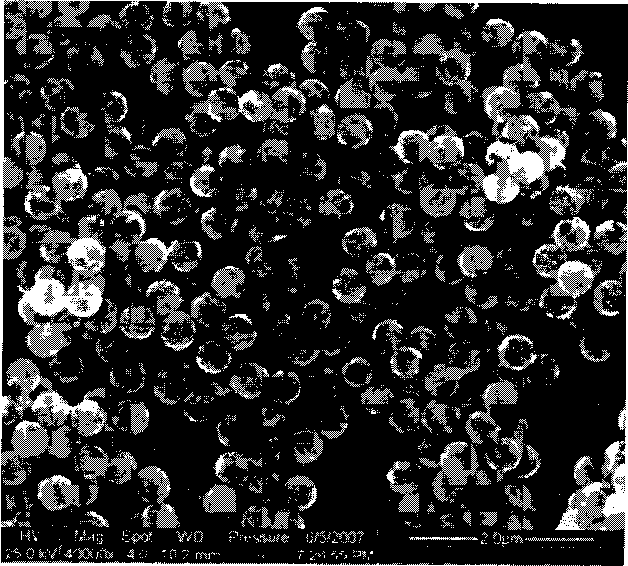
[0038] with FeCl 3 / EtOH solution acts as a catalyst precursor with a concentration of 1mmol / L. The selected carrier includes silica microspheres (about 400nm in particle size) and porous magnesia. Soak 0.05g of carrier powder in 20ml of the above-mentioned FeCl 3 / EtOH solution for 30 minutes, centrifuge to discard the liquid part, and dry the solid powder at 70°C;

[0039] The reaction chamber is sealed, and argon gas is introduced to exhaust the air;

[0040] The temperature was raised to 900°C, and 100 sccm of hydrogen gas was used to reduce the catalyst particles for 20 minutes;

[0041] 2. Chemical vapor deposition

[0042] Keep the temperature constant, turn off the hydrogen used for reduction, and change it to 800-1000 sccm argon to act as a dilue...

Embodiment 2

[0046] Embodiment 2: Surface Random film growth of semiconducting single-walled carbon nanotubes of the present invention

[0047] This embodiment adopts the same device and steps as in Example 1, the difference is that the substrate is replaced with a silicon wafer with a 400nm thick oxide layer, and the catalyst precursor solution is dropped on the substrate and dried quickly so that it is evenly covered on the silicon wafer. A thin film of catalyst particles was formed on the surface of the sheet.

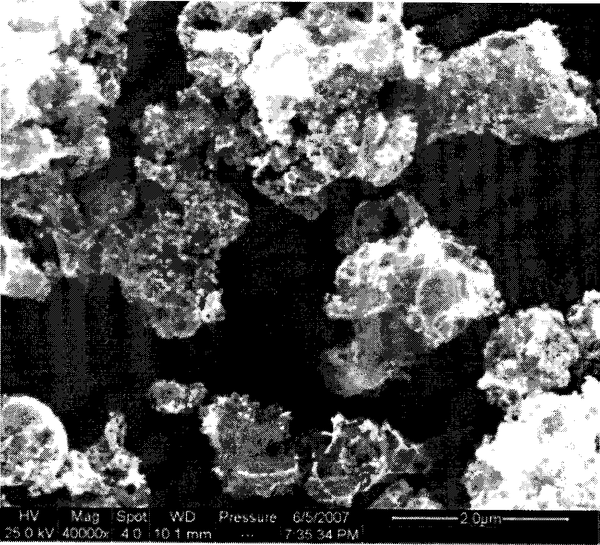
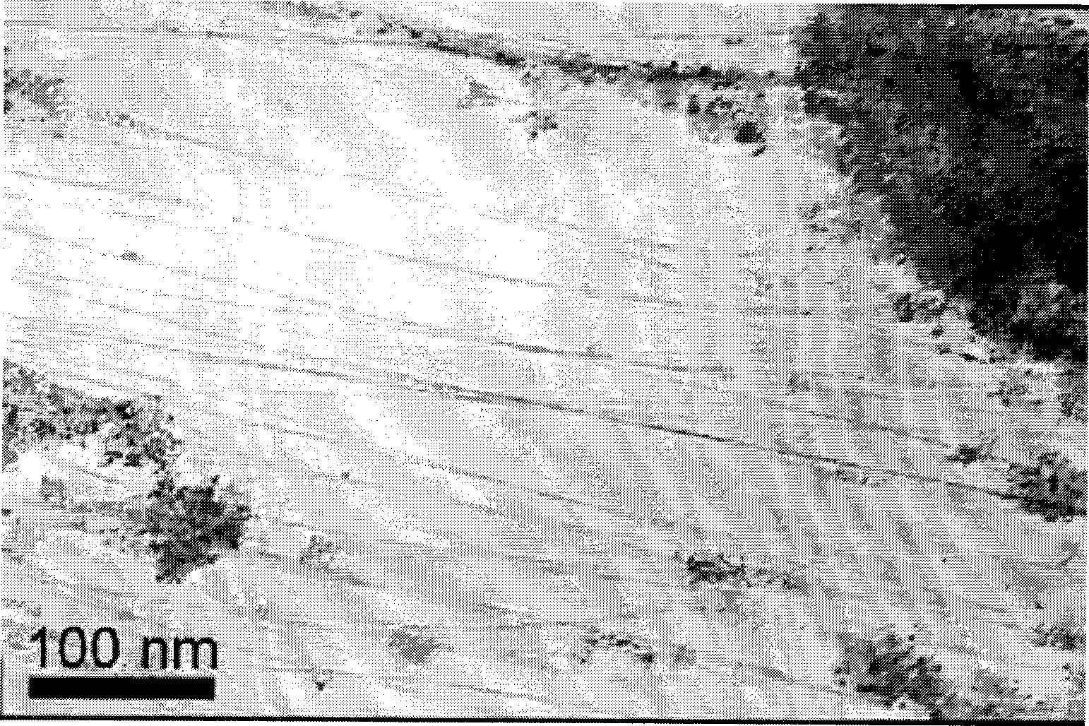
[0048] The scanning electron micrograph of the semiconductor-type single-walled carbon nanotube obtained in the present embodiment is as attached Figure 4 As shown, the XPS spectrum is as Image 6 As shown, the Raman spectrum is shown as Figure 7 As shown, its RBM is located at 157.3cm -1 , is a single-walled carbon nanotube with a diameter of about 1.6nm. The height of the D Band peak is not high, which shows that a good quality single-walled carbon nanotube film can be o...

Embodiment 3

[0049] Example 3: Surface Oriented Array Growth of Semiconducting Single-walled Carbon Nanotubes of the Present Invention

[0050] 1. Preparation of catalyst

[0051] Catalyst is prepared according to the same method as in Example 1, the difference is that the catalyst precursor solution is applied to the front end of the silicon chip;

[0052] 2. Chemical vapor deposition

[0053] Then keep the temperature constant, turn off the hydrogen used for reduction, and change it into 800-1000 sccm argon to serve as a diluent gas;

[0054] Pull the reaction area out of the constant temperature area for 5 minutes, so that the temperature of the reaction area is about 300°C different from the constant temperature area in the furnace; introduce the pyridine vapor generated by bubbling 10.0 sccm of hydrogen into the reaction system, and pull the reaction area back to the constant temperature in the furnace Zone, 900°C constant temperature for 15 minutes; during the reaction process, pla...


PUM

PropertyMeasurementUnit
Particle sizeaaaaaaaaaa

Abstract

The invention discloses a semiconductor-typed single-walled carbon nano tube and a preparation method thereof, belonging to the carbon nano tube technical field. The carbon atoms on the tube wall of the single-walled carbon nano tube are replaced by doping atoms which comprise nitrogen atoms, boron atoms, oxygen atoms or sulfur atoms. The preparation method thereof comprises: at the reaction temperature, in an inert environment and under the catalysis of a catalyst which is positioned on substrate, the reaction gas is deposited on the substrate by chemical vapor deposition, so as to obtain the carbon nano tube; the reaction gas comprises carbon source and doped source which come from the same substance or different substances; after the chemical vapor deposition, a semiconductor-typed single-walled carbon nano tube is prepared. Compared with the prior art, the invention has the advantages of simple equipment, easy operation, low raw material cost and strong product repeatability, and can obtain single-walled carbon nano tubes which are all semiconductor-typed.

Description

technical field [0001] The invention relates to a semiconducting single-wall carbon nanotube and a preparation method thereof, in particular to a method for preparing a semiconducting single-wall carbon nanotube by doping other elements in a chemical vapor deposition reaction, and belongs to the technical field of carbon nanotubes. Background technique [0002] How to detect and manipulate the atomic-scale microcosm has always been the direction that scientists in various fields are striving to explore. In the past few decades, the rapid development of nanotechnology has made people continue to make progress in this direction. Research on nanomaterials and nanotechnology has been widely carried out from basic disciplines such as physics, chemistry, and biology to applied disciplines such as materials, machinery, electronics, medicine, and energy. It can be said that nanotechnology is leading a new technological revolution, and it has gradually entered the life vision of ord...

Claims


Application Information

Patent Timeline
IPC IPC(8): C01B31/02
Inventor 李彦刘宇金钟
Owner PEKING UNIV
Why Eureka
Try Eureka