Magnetic and dielectric composite electronic device

a composite electronic device and dielectric technology, applied in the direction of magnetic body, fixed capacitor details, printed circuit non-printed electric components association, etc., can solve the problems of power loss, composite device using a single material is limited in performing various functions, and cannot meet the requirements of diverse small application machines

Inactive Publication Date: 2009-04-16
CERATECH
View PDF6 Cites 52 Cited by
  • Summary
  • Abstract
  • Description
  • Claims
  • Application Information

AI Technical Summary

Problems solved by technology

However, since mounting an individual device increases an area for the mounting, it does not meet the requirements for diverse small application machines.
However, a composite device using a single material is limited in performing various functions.
However, this filter has the problems of signals generated by a resistance element, power loss and a complicate manufacturing process.
However, when the magnetic material and the dielectric material are joined together and thermally treated at a high temperature, since interdiffusion is generated between the different materials during a firing process, the composite component has the problems in that electrical characteristics and durability of the final device deteriorate.
Moreover, when multilayered different materials undergo co-firing process, it is difficult to match firing shrinkage between the different materials.
Thus, compared to the manufacturing of each component using a single material, it is very difficult to control the conditions of a manufacturing process of the composite device.
Consequently, when a single composite device is manufactured by forming the different materials to be integrally with each other, there are many problems in that it is difficult to secure stabilized characteristics of the device, a yield is not good and a manufacturing cost increases.
Therefore, there are many problems to be solved with respect to the reliability of the device and the productivity thereof.

Method used


Image

  • Magnetic and dielectric composite electronic device
  • Magnetic and dielectric composite electronic device
  • Magnetic and dielectric composite electronic device

Examples


first embodiment

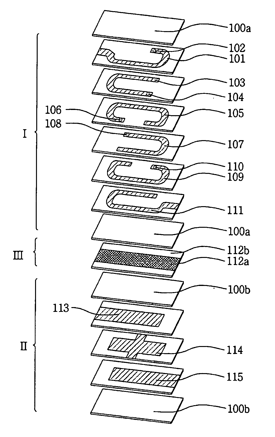
[0046]FIG. 1 is an exploded perspective view of a composite electronic device according to the present invention. In the composite electronic device, a third region III is interposed as the middle layer between a first region I in which a plurality of magnetic material sheets 100a are layered and a second region II in which a plurality of dielectric material sheets 100b are layered. The first region I corresponds to the inductor and the second region II corresponds to the varistor. The middle layer interposed between the first region I and the second region II includes a Zn—Ti-based material to prevent the diffusion of the materials when the first region I and the second region II undergo co-firing process.

[0047]The first region I, the second region II and the third region III are layered to one another, to be integrally formed in a single body, and then, is completed as a chip-type electronic device having an electrode terminal formed on an outer surface as described later.

[0048]Th...

second embodiment

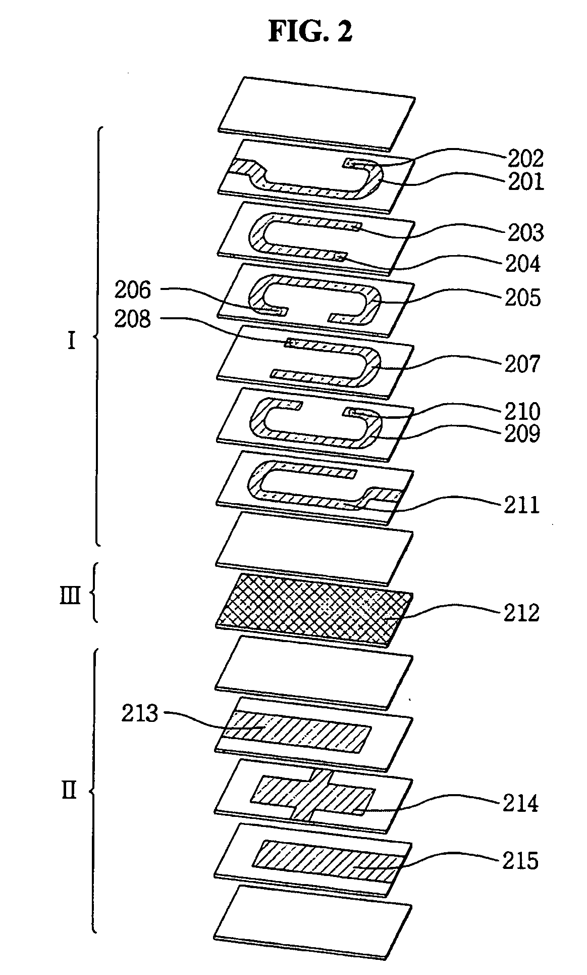
[0051]In FIG. 1, the third region III is formed of the composite sheet including a central part 112a formed of the Zn—Ti-based material and an edge part 112b formed of the magnetic material or the dielectric material. However, in accordance with FIG. 2, a third region III is formed of a Zn—Ti-based material formed on a whole sheet 212. An area of the middle layer occupied by the Zn—Ti-based material forming the third layer III may vary in consideration of adhesion characteristics of the composite electronic device, any shrinkage during firing process, and the like.

third embodiment

[0052]FIG. 3 is an exploded perspective view of an electronic device according to the present invention. A third region III is interposed as a middle layer between a first region I in which a plurality of magnetic material sheets 300a are layered and a second region II in which a plurality of dielectric material sheets 300b are layered. The middle layer interposed between the first region I and the second region II includes a Zn—Ti-based material of preventing the diffusion of the materials when the first region I and the second region II are co-fired.

[0053]Unlike the foregoing two embodiments, in the first region I of the third embodiment, as shown in FIG. 3, a plurality of respective electrode patterns 301, 303, 305, 307, 309 and 311 are respectively formed to be independent from one another on at least at parts of the plurality of magnetic material sheets 300a formed of the magnetic material. Respective via-holes 302, 304, 306, 308 and 310 are formed at the ends of the respective...


PUM


Abstract

There is a provided a magnetic and dielectric composite electronic device, comprising: a first region with a plurality of magnetic material sheets being layered; a second region with a plurality of dielectric material sheets being layered; and a third region as a middle layer interposed between the first region and the second region, including a Zn—Ti based material to prevent diffusion of the materials during co-firing of the first region and the second region, and the first region, the second region and the third region are integrally formed in a single body. In accordance with the present invention, the low pass filter including the function of the varistor is realized to obtain the EMI function and the ESD control effect. Furthermore, the one chip electronic device having the composite functions is manufactured by a simple process, and the interdiffusion between the different materials forming the magnetic and the dielectric parts is prevented to secure the durability and electrical characteristics of the product.

Description

RELATED APPLICATIONS[0001]The present application claims priority from Korean Patent Application No. 2007-104111, filed Oct. 16, 2007, the contents of which are incorporated herein by reference in their entirety.FIELD OF THE INVENTION[0002]The present invention relates to a magnetic and dielectric composite electronic device, and more particularly, to a multilayered chip-type electronic device in which a magnetic material functioning as an inductor is formed integrally with a dielectric material functioning as a capacitor and a varistor.BACKGROUND OF THE INVENTION[0003]A resistor R, a capacitor C and an inductor L, which are used as passive devices in an electronic circuit, may have their respective typical functions and roles but may be combined together, to perform a new circuit function. For example, a capacitor basically interrupts a direct current and allows an alternating current signal to pass but it may form a time constant circuit, a time delay circuit, an RC filter and an ...

Claims


Application Information

Patent Timeline
Patent Type & Authority Applications(United States)
IPC IPC(8): H05K1/16H05K1/03
CPCH01F1/344H01F17/0013H03H2001/0085H01G4/40H03H7/0107H01F2017/0066H01C7/10H01F17/03H01G4/30
Inventor CHO, KYOUNG HWANSONG, JUNG IKCHOI, JEONG IN
Owner CERATECH
Why Eureka
Try Eureka