Methods of Forming Integrated Circuit Devices Having Ion-Cured Electrically Insulating Layers Therein

a technology of ion-cured electrical insulation and integrated circuit, which is applied in the manufacture of basic electric elements, semiconductor/solid-state devices, electric devices, etc., can solve problems such as deformation of insulating materials used to fill gaps, and achieve the effects of improving device isolation regions, reducing atomic order, and increasing atomic order

Active Publication Date: 2009-04-16
IBM CORP +2
View PDF1 Cites 184 Cited by
  • Summary
  • Abstract
  • Description
  • Claims
  • Application Information

AI Technical Summary

Benefits of technology

[0004]Methods of forming an integrated circuit device according to embodiments of the present invention utilize ion implantation and annealing techniques to improve the quality of device isolation regions (e.g., trench isolation regions) within an integrated circuit substrate. Methods according to some of these embodiments include forming a trench in a surface of semiconductor substrate and filling the trench with an electrically insulating region having a seam therein. The trench may be filled by depositing a sufficiently thick electrically insulating layer on sidewalls and a bottom of the trench. Curing ions are then implanted into the electrically insulating region at a sufficient energy and dose to reduce a degree of atomic order therein. The curing ions may be ones selected from a group consisting of nitrogen (N), phosphorus (P), boron (B), arsenic (As), carbon (C), argon (Ar), germanium (Ge), helium (He), neon (Ne) and xenon (Xe). These curing ions may be implanted at an energy of at least about 80 KeV and a dose of at least about 5×10¹⁴ ions / cm2. The electrically insulating region is then annealed at a sufficient temperature and for a sufficient duration to increase a degree of atomic order within the electrically insulating region.

Problems solved by technology

When a gap is filled during the deposition of an insulating film, an increase in the aspect ratio of the gap may cause defects in the insulating material used to fill the gap.
However, since the HDP oxide film is formed by a high-density plasma, plasma attack against lower patterns (for example, gate electrode patterns) may be caused by the high-density plasma.

Method used


Image

  • Methods of Forming Integrated Circuit Devices Having Ion-Cured Electrically Insulating Layers Therein
  • Methods of Forming Integrated Circuit Devices Having Ion-Cured Electrically Insulating Layers Therein
  • Methods of Forming Integrated Circuit Devices Having Ion-Cured Electrically Insulating Layers Therein

Examples


Embodiment Construction

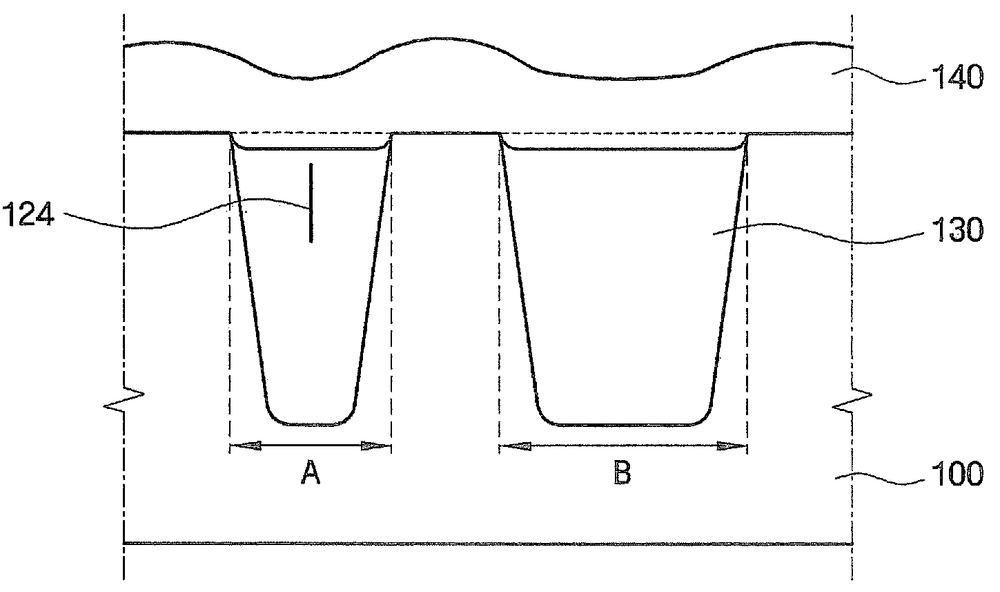
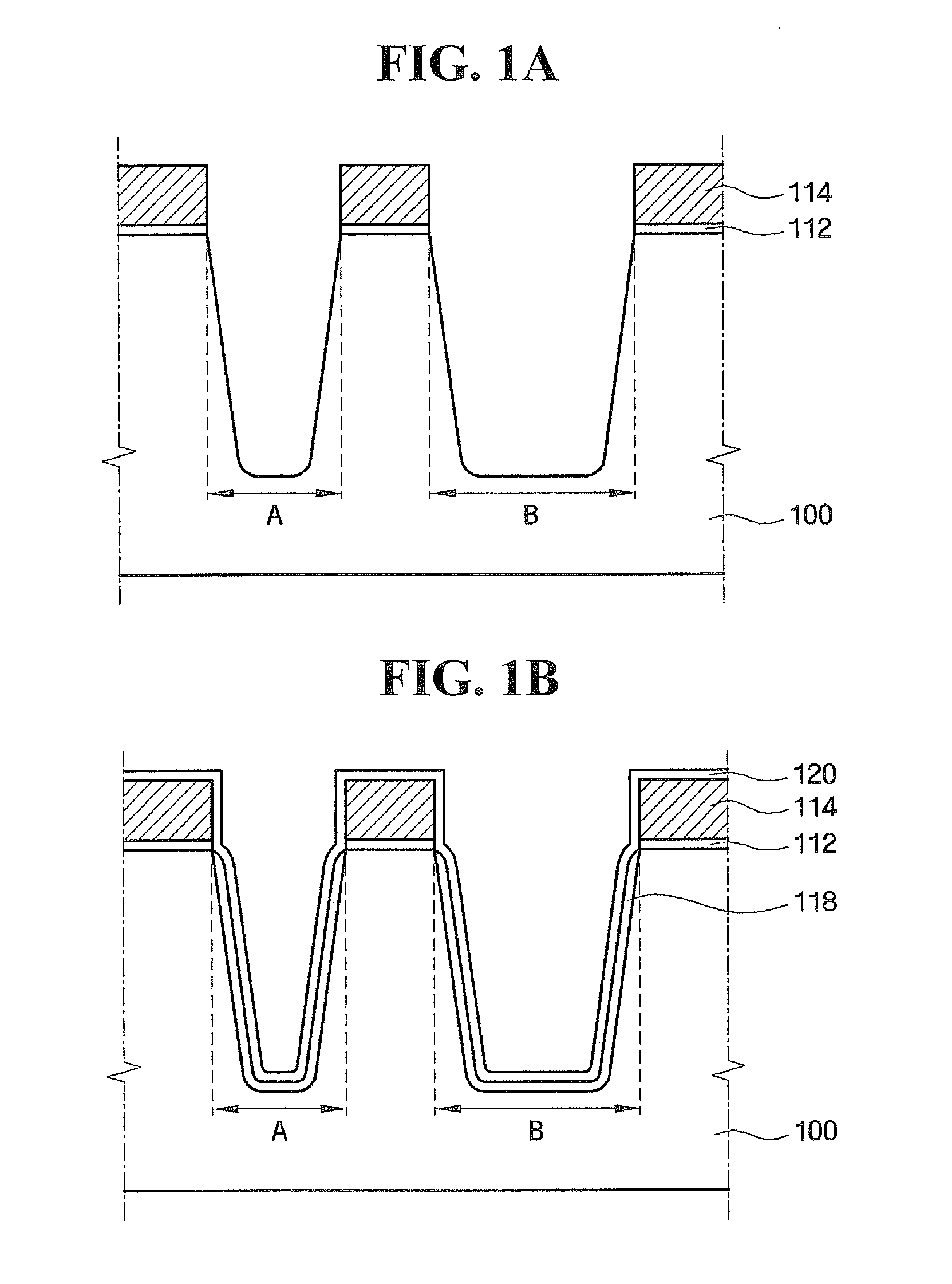
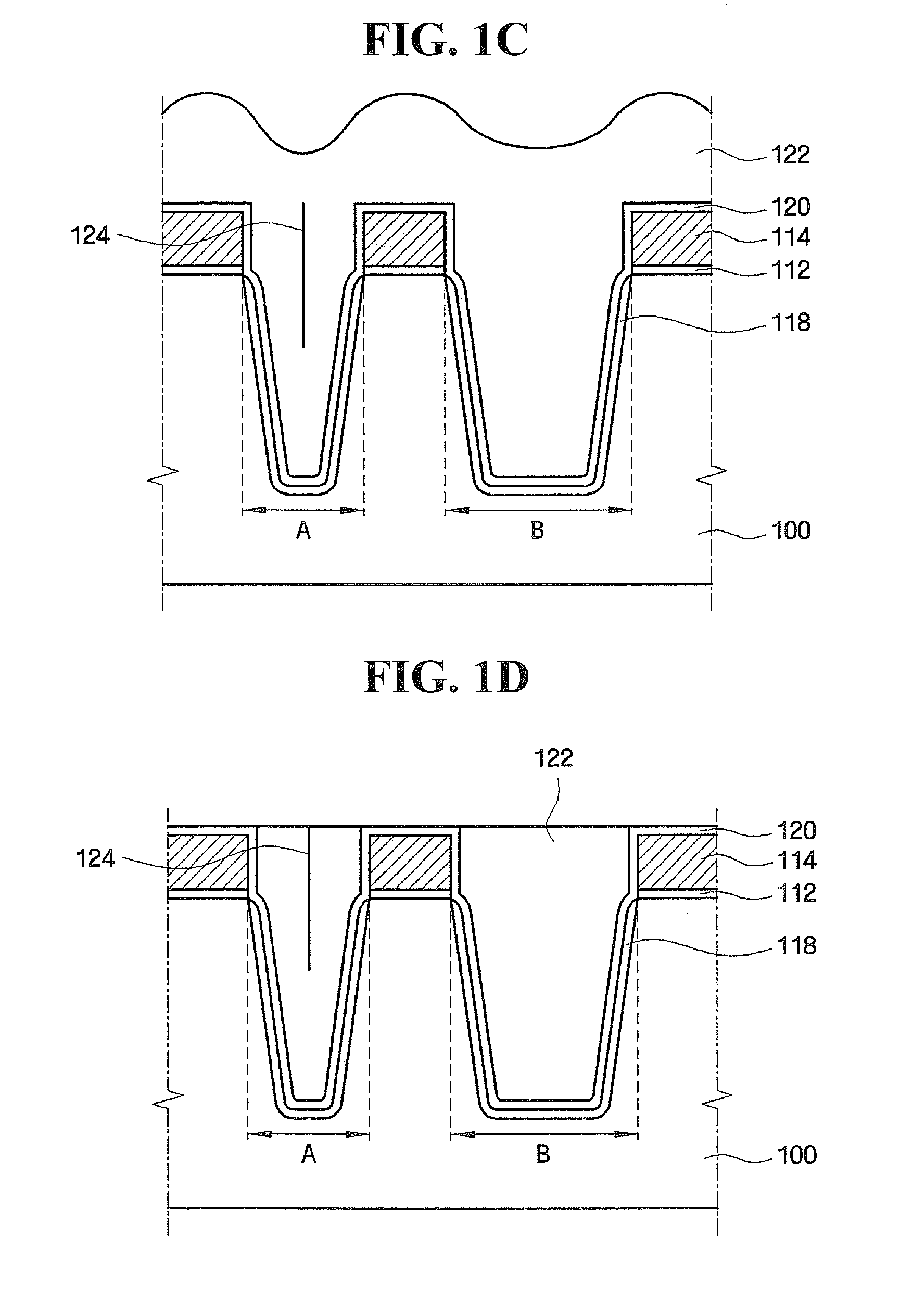
[0011]Advantages and features of the present invention and methods of accomplishing the same may be understood more readily by reference to the following detailed description of preferred embodiments and the accompanying drawings. The present invention may, however, be embodied in many different forms and should not be construed as being limited to the embodiments set forth herein. Rather, these embodiments are provided so that this disclosure will be thorough and complete and will fully convey the scope of the invention to those skilled in the art. Like reference numerals refer to like elements throughout the specification.

[0012]The term “and / or” includes any and all combinations of one or more of the associated listed items. As used herein, the singular forms “a”, “an” and “the” are intended to include the plural forms as well, unless the context clearly indicates otherwise. It will be further understood that the terms “comprises” and / or “comprising,” when used in this specificati...


PUM


Abstract

Methods of forming integrated circuit devices include forming a trench in a surface of semiconductor substrate and filling the trench with an electrically insulating region having a seam therein. The trench may be filled by depositing a sufficiently thick electrically insulating layer on sidewalls and a bottom of the trench. Curing ions are then implanted into the electrically insulating region at a sufficient energy and dose to reduce a degree of atomic order therein. The curing ions may be ones selected from a group consisting of nitrogen (N), phosphorus (P), boron (B), arsenic (As), carbon (C), argon (Ar), germanium (Ge), helium (He), neon (Ne) and xenon (Xe). These curing ions may be implanted at an energy of at least about 80 KeV and a dose of at least about 5×10¹⁴ ions/cm2. The electrically insulating region is then annealed at a sufficient temperature and for a sufficient duration to increase a degree of atomic order within the electrically insulating region.

Description

FIELD OF THE INVENTION[0001]The present invention relates to integrated circuit fabrication methods and, more particularly, to methods of fabricating integrated circuits that utilize trench isolation regions therein.BACKGROUND OF THE INVENTION[0002]In a semiconductor device, a plurality of unit elements such as transistors, bit lines, or metal wires can be integrated into a substrate. The plurality of unit elements should often be insulated from one another. An insulating film can be used to insulate the unit elements from one another, and an oxide film has been used as a typical insulating film. A BPSG (Boro Phospho Silicate Glass) film, a BSG (Boro Silicate Glass) film, a PSG (Phospho Silicate Glass) film, a TEOS (Tetra Ethyl Ortho Silicate) film, an USG (Undoped Silicate Glass) film, or a combination thereof have also been used as insulating films.[0003]Due to a high degree of integration of the semiconductor device, a distance between patterns thereon is decreased and a height o...

Claims


Application Information

Patent Timeline
Patent Type & Authority Applications(United States)
IPC IPC(8): H01L21/762
CPCH01L21/3105H01L21/76232H01L21/76229H01L21/762
Inventor KIM, JUN-JUNGKIM, JOO-CHANPARK, JAE-EONCONTI, RICHARD ANTHONYLUN, ZHAOWIDODO, JOHNNYWILLE, WILLIAM C.ZUO, BIAO
Owner IBM CORP
Why Eureka
Try Eureka