Electronic device and manufacturing method thereof

a manufacturing method and electronic component technology, applied in the manufacture of printed circuits, printed circuit aspects, basic electric elements, etc., can solve the problems of difficult to form desired shapes of conductive resin (conductive adhesive), which is a mixture of metal particles and resin, and the risk of damage to the electrical connection part, so as to prevent short circuit between adjacent bumps, reduce stress, and prevent damage to the bump

Inactive Publication Date: 2009-04-23
NEC CORP
View PDF2 Cites 7 Cited by
  • Summary
  • Abstract
  • Description
  • Claims
  • Application Information

AI Technical Summary

Benefits of technology

[0023]According to present invention, even if the conductive resin is used in the flip chip mounting of the electronic component with the substrate, a short circuit between adjacent bumps can be prevented because the flow of the conductive resin at the time of the flip chip mounting is restrained by the recess and the sheet.
[0024]A

Problems solved by technology

The conductive resin (conductive adhesive) which is a mixture of metal particles and resin is difficult to form a desired shape at the time of the flip chip mounting.
If a pad is formed on a flat surface of a substrate, there is a risk of a short circuit between adjacent pads because the conductive resin spreads around the pad when an electronic component is connected with the substrate electrically.
However, if the bump is in contact with the electrode on t

Method used


Image

  • Electronic device and manufacturing method thereof
  • Electronic device and manufacturing method thereof
  • Electronic device and manufacturing method thereof

Examples


Embodiment Construction

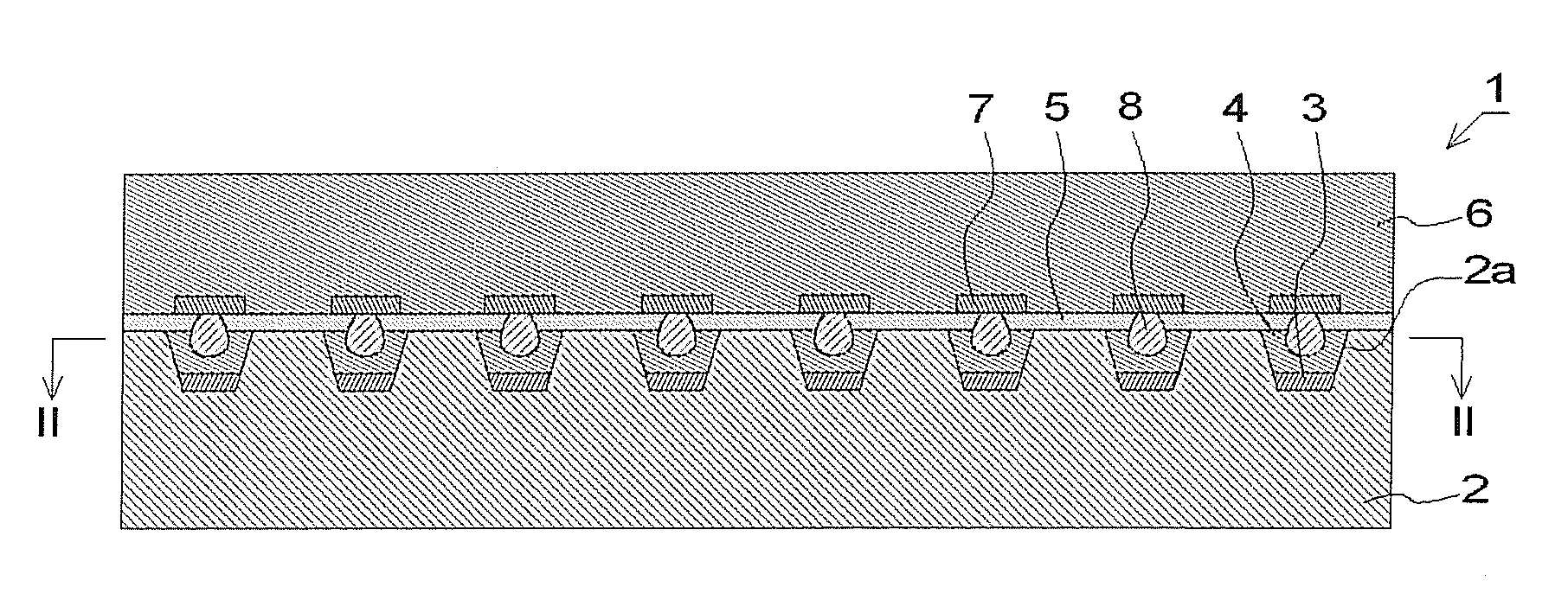
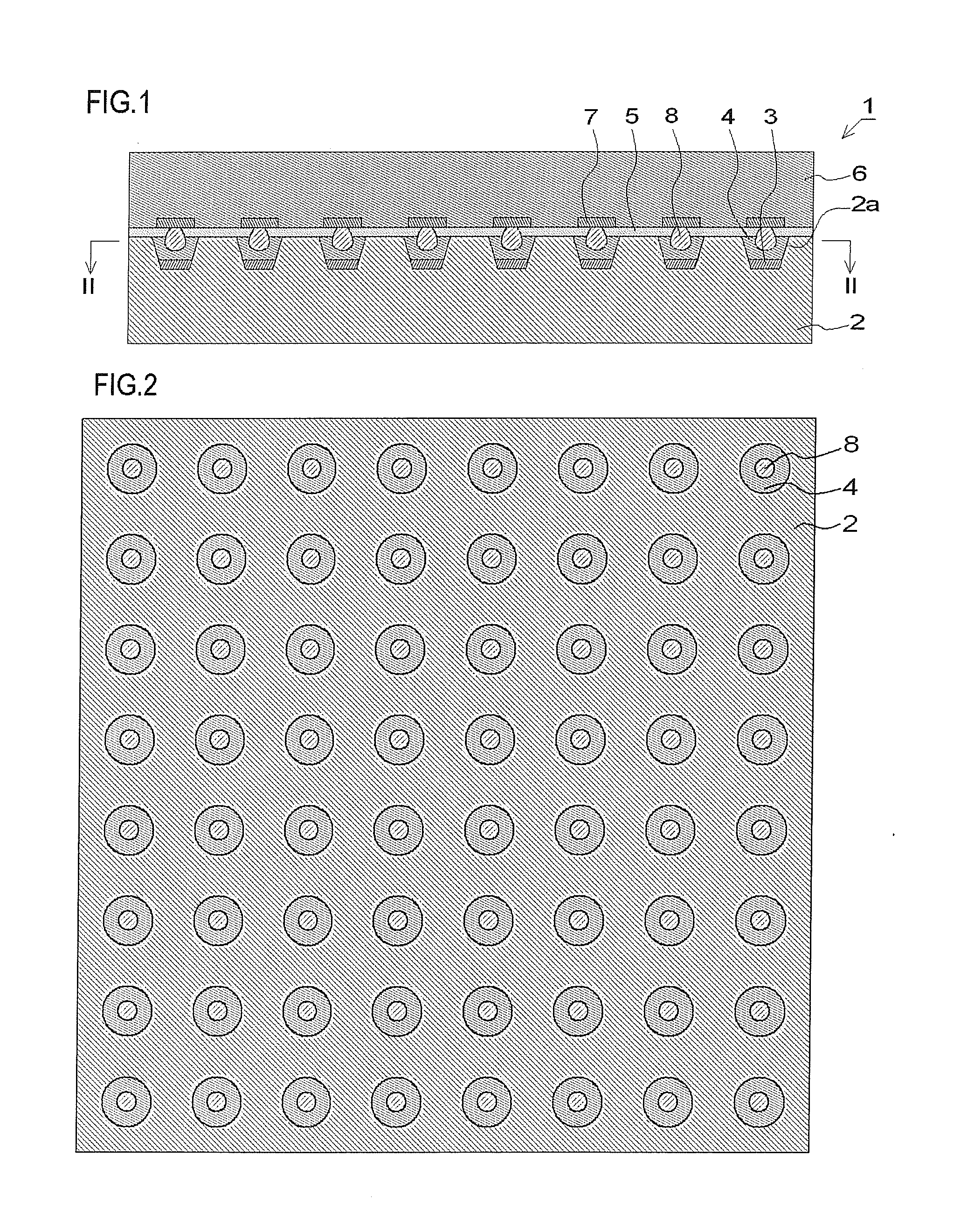
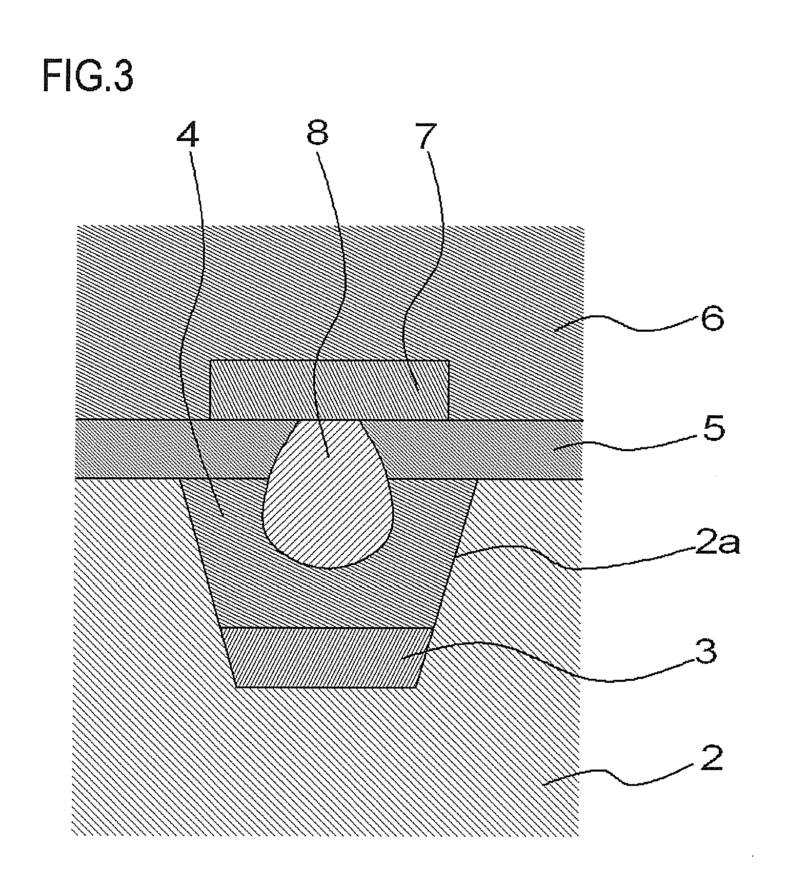
[0030]An electronic device will be explained by giving an example of a semiconductor device. FIG. 1 shows a schematic and cross-sectional view of the electronic device of an exemplary embodiment of the semiconductor device. FIG. 2 shows a schematic and cross-sectional view along a II-II line in FIG. 1. FIG. 3 shows a schematic and cross-sectional view enlarging an electrical connection part between an electronic component and a substrate. The electronic device 1 is a semiconductor device in which a semiconductor component 6 as the electronic component is mounted on a substrate 2 by flip chip bonding. In the substrate 2, recesses (or reentrants) 2a are formed on a surface opposite to the semiconductor component 6. At least one first pad (electrode) 3 for being electrically connected with the semiconductor component 6 is formed on the bottom (surface) of the recess 2a. A bump 8 formed on a second pad 7 of the semiconductor component 6 is connected with the first pad 3 of the substrate...


PUM


Abstract

Electronic device has substrate having at least one pad, electronic component having bump connected with pad of substrate electrically and mounting on substrate by flip chip bonding, conductive resin electrically connecting pad with bump, and insulation sheet disposed between substrate and electronic component. Substrate has recess on surface opposite to electronic component. Pad is formed on recess bottom. Conductive resin is provided on pad and in recess. Sheet has through hole corresponding to each bump. Opening area of through hole is smaller than that of recess. Bump is inserted into through hole, in contact with inner wall of through hole, electrically connected with pad via conductive resin, without direct contact with pad.

Description

REFERENCE TO RELATED APPLICATION[0001]This application is based upon and claims the benefit of the priority of Japanese patent application No. 2007-275318, filed on Oct. 23, 2007, the disclosure of which is incorporated herein in its entirety by reference thereto.TECHNICAL FIELD[0002]This invention relates to an electronic device mounting a electronic component, and a manufacturing method thereof. The invention relates to a semiconductor device mounting a semiconductor component as the electronic component by flip chip bonding and, a method of manufacturing the semiconductor device, for example.BACKGROUND[0003]In recent years, for an electric bonding between an electronic component such as a semiconductor component and a substrate, lead-free solder is used mainly. Because of the high melting point of the lead-free solder, a solder-bonding process at high temperature is necessary. At the time of the mounting, therefore, it is necessary to pay attention to heat load on the substrate a...

Claims


Application Information

Patent Timeline
IPC IPC(8): H01L23/488H01L21/60
CPCH01L24/16H01L2224/83192H01L2224/0401H01L2224/10175H01L2224/13099H01L2224/16237H01L2224/81385H01L2224/81897H01L2924/01082H05K3/321H05K2201/09472H05K2201/10575H05K2201/10674H01L24/81H01L2224/81191H01L2924/01005H01L2924/01006H01L2924/01019H01L2924/01047H01L2924/00014H01L2224/13023H01L2224/16111H01L2924/3841
Inventor HORI, EIJI
Owner NEC CORP
Why Eureka
Try Eureka