Method for Validating Printed Circuit Board Materials for High Speed Applications

a printed circuit board and high-speed technology, applied in the direction of heat measurement, optical radiation measurement, instruments, etc., can solve the problems of high level of skill, high cost, and approach taken to qualify materials for pcbs, and achieve the effect of short propagation pulse or corner-corner probing, and high level of equipmen

Inactive Publication Date: 2009-04-23
IBM CORP
View PDF9 Cites 14 Cited by
  • Summary
  • Abstract
  • Description
  • Claims
  • Application Information

AI Technical Summary

Benefits of technology

[0009]One embodiment of the present invention provides a method for testing a printed circuit board. The method applies a high frequency electronic signal, most preferably a microwave frequency, to an electronically conductive microstrip embedded within the printed circuit board. The temperature at the surface of the printed circuit board adjacent the embedded microstrip is measured and compared to a setpoint temperature representative of a standard acceptable printed circuit board. Optionally, the microwave signal may be generated using a PCI Express controller chip or a function ge

Problems solved by technology

At such high speeds, the electronic communications through the bus are subject to dielectric dissipation factor, also known as dielectric loss.
Present approaches ta

Method used


Image

  • Method for Validating Printed Circuit Board Materials for High Speed Applications
  • Method for Validating Printed Circuit Board Materials for High Speed Applications
  • Method for Validating Printed Circuit Board Materials for High Speed Applications

Examples


Embodiment Construction

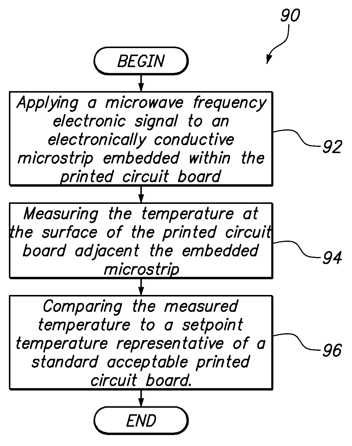
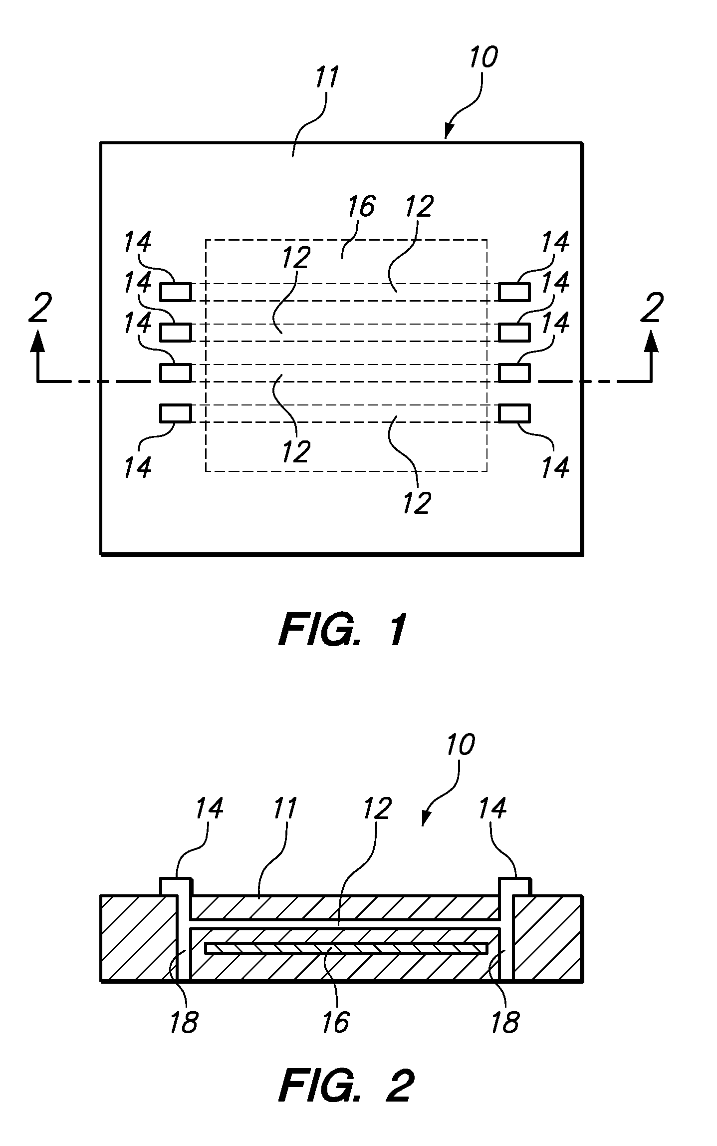
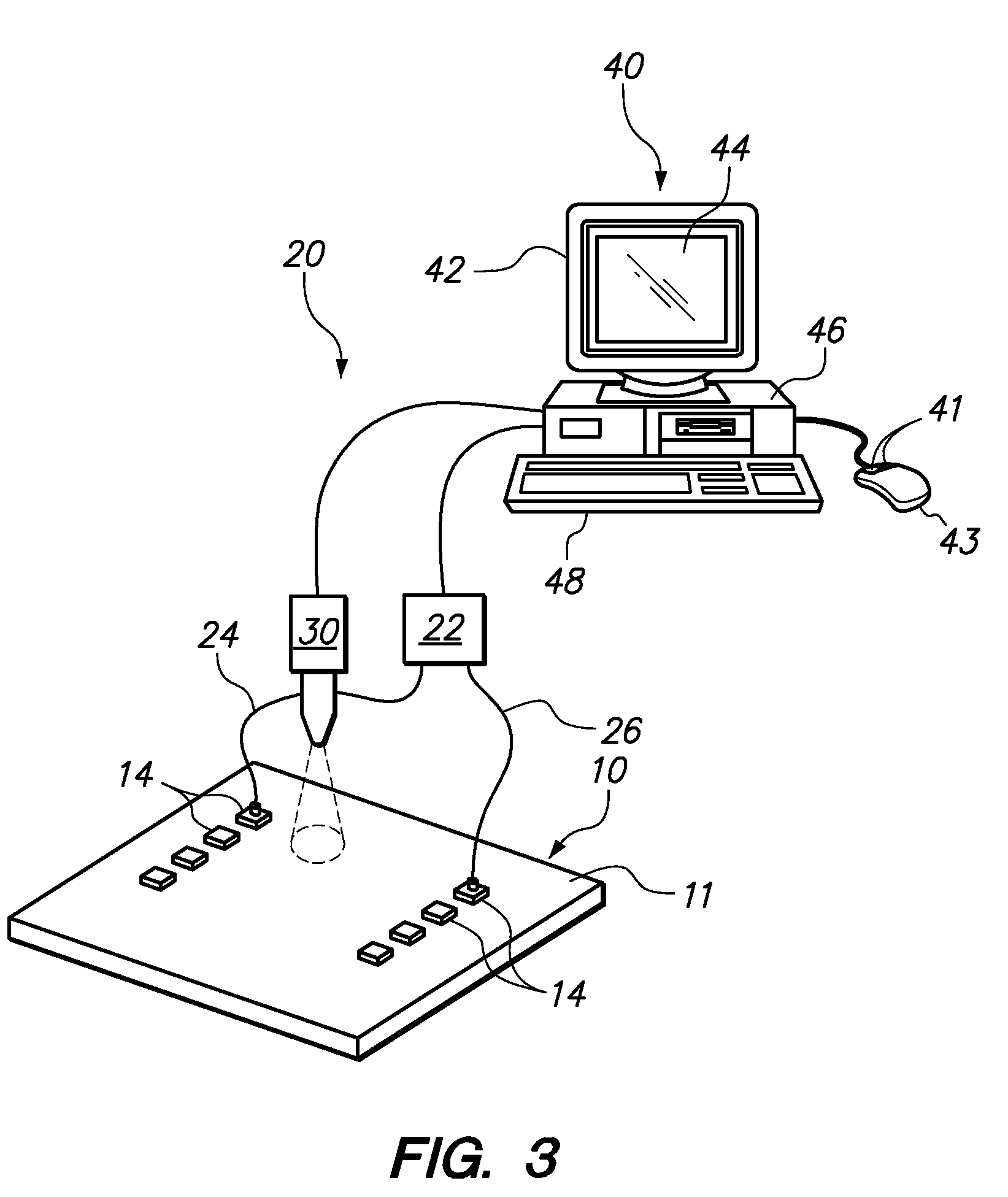
[0015]One embodiment of the present invention provides a method for testing a printed circuit board. The test is beneficial in determining the extent of dielectric loss associated with the material used to make the printed circuit board. When a high frequency electronic signal is communicated through a microstrip that is embedded within the printed circuit board, dielectric losses generate heat that is measurable by an increase in the temperature at the surface of printed circuit board. Comparing the measured temperature or temperature spectrum against the temperature or spectrum of an acceptable standard printed circuit board provides a quick and simple determination whether the material used in the tested printed circuit board is acceptable.

[0016]In a specific embodiment, the method applies a high frequency electronic signal to an electronically conductive microstrip embedded within the printed circuit board. The high frequency signal is preferably applied at a microwave frequency...


PUM


Abstract

A method for testing a printed circuit board to determining the dielectric loss associated with the circuit board material relative to a standard. Dielectric losses in the material generate heat when a high frequency electronic signal, such as a microwave frequency signal, is communicated through a microstrip that is embedded within the printed circuit board. The temperature or spectrum at the surface of printed circuit board is measured and compared against the temperature or spectrum of the standard to determine whether the material under test is acceptable. While various temperature measurement devices may be used, the temperature is preferably measured without contacting the surface, such as using an infrared radiation probe.

Description

BACKGROUND OF THE INVENTION[0001]1. Field of the Invention[0002]The present invention relates to methods of testing printed circuit board materials for applications involving high-speed communications.[0003]2. Description of the Related Art[0004]A printed circuit board (PCB) is used to mechanically support and electrically connect electronic components using conductive pathways, or traces, etched from copper sheets that have been laminated onto a non-conductive substrate. Populating the board with electronic components forms a printed circuit assembly (PCA), also known as a printed circuit board assembly (PCBA). PCBs are rugged, inexpensive, and can be highly reliable. They require more initial layout effort than either wire-wrapped or point-to-point constructed circuits, but are much cheaper, faster, and consistent in high volume production. Many aspects of PCB design, assembly, and quality control are set by standards that are published by the IPC organization[0005]Some PCBs have ...

Claims


Application Information

Patent Timeline
IPC IPC(8): G01R31/02G01K3/00G01N25/72
CPCG01J5/0096G01N25/72G01R31/309G01R31/2837G01R31/2818
Inventor CASES, MOISESHERRMAN, BRADLEY DONALDHOWIESON, KENT BARCLAYMATOGLU, ERDEMMUTNURY, BHYRAV MURTHYPATEL, PRAVINPHAM, NAM HUUWESLEY, CELEB JAMES
Owner IBM CORP
Why Eureka
Try Eureka