Patterning process

a technology of patterning and process, applied in the field of patterning process, can solve the problems of complex process procedure and reduced throughput, and achieve the effect of simplifying the process procedur

Inactive Publication Date: 2009-04-23
MACRONIX INT CO LTD
View PDF5 Cites 13 Cited by
  • Summary
  • Abstract
  • Description
  • Claims
  • Application Information

AI Technical Summary

Benefits of technology

[0006]Accordingly, the present invention is to provide a method for patterning a material layer capable of simplifying the process procedure.

Problems solved by technology

However, in the conventional double patterning process, the etching process should be performed several times. Therefore, the process procedure is complex and the throughput is decreased.

Method used


Image

  • Patterning process
  • Patterning process
  • Patterning process

Examples


Embodiment Construction

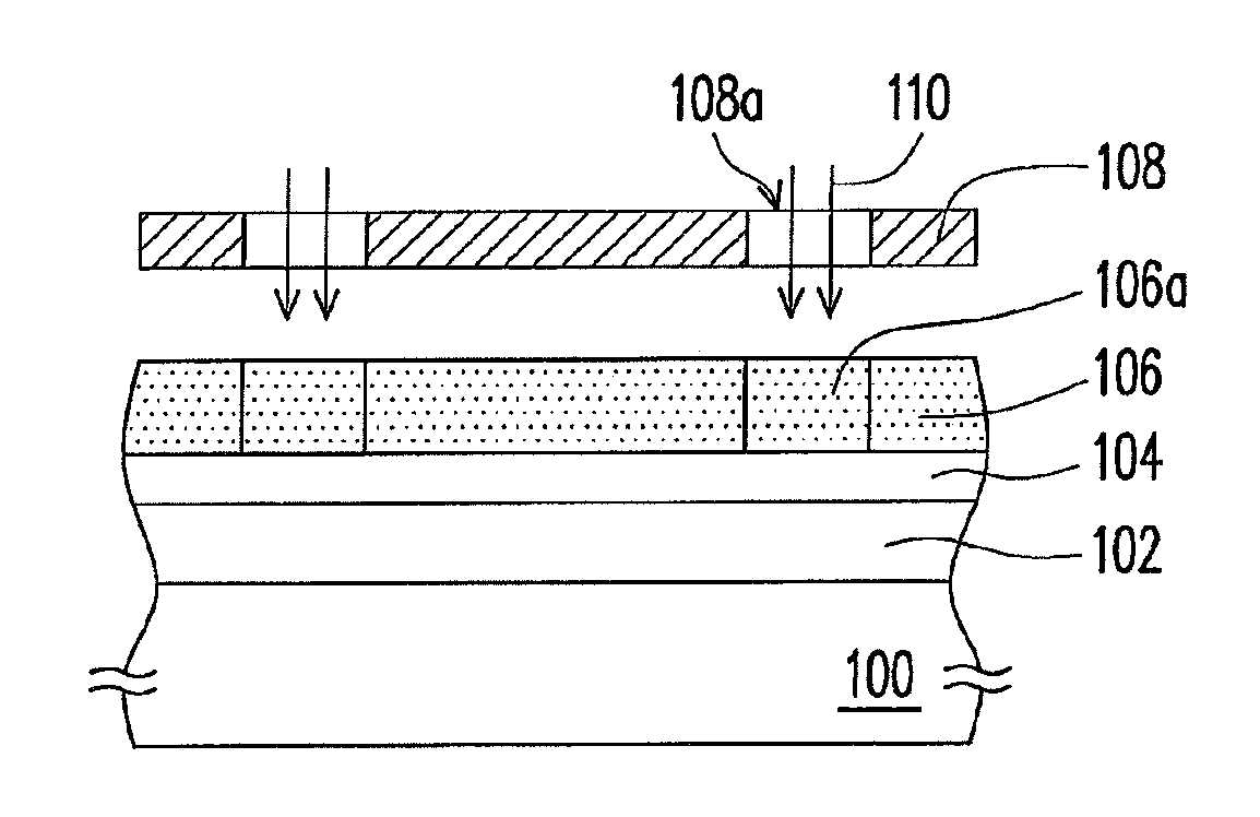
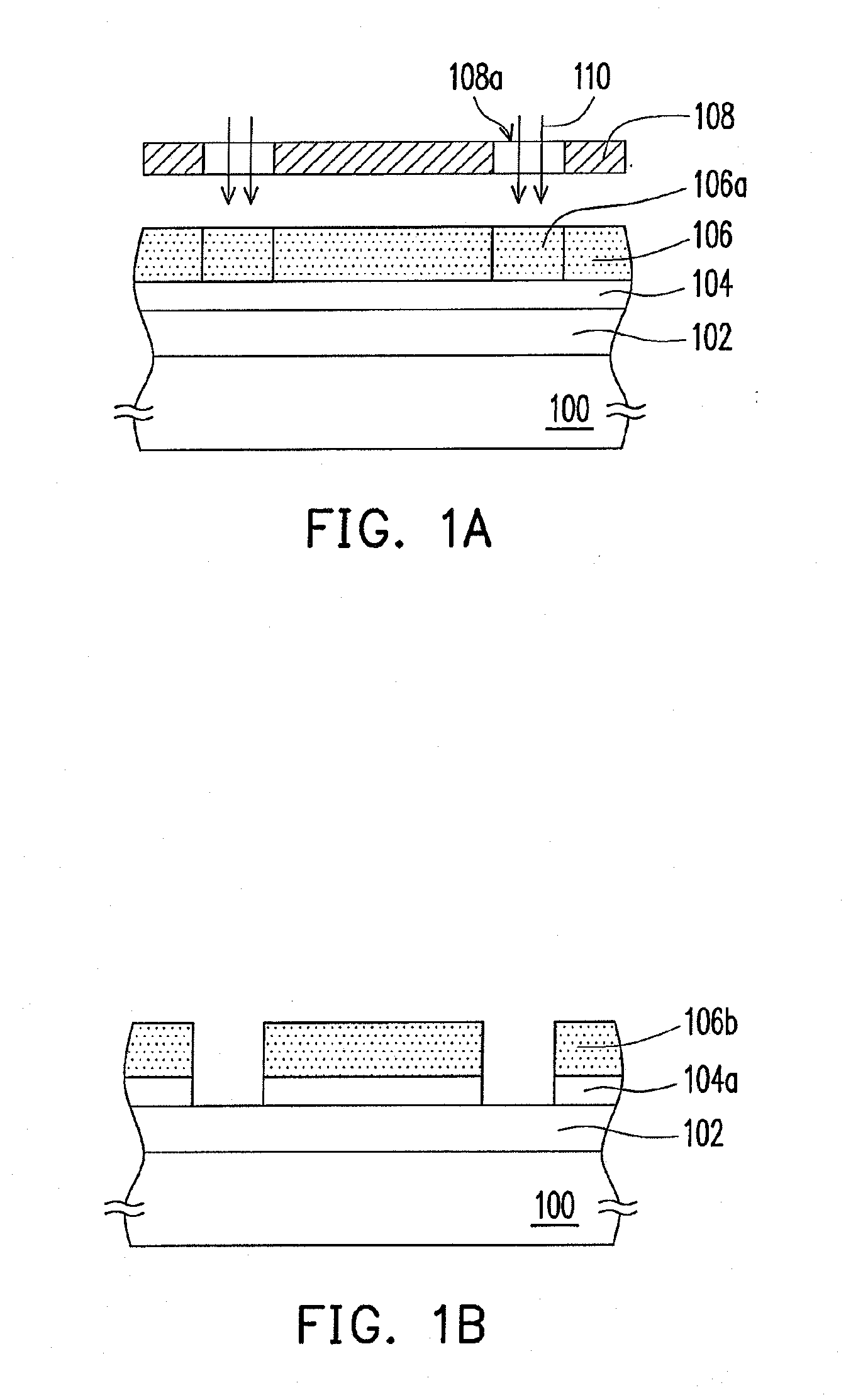
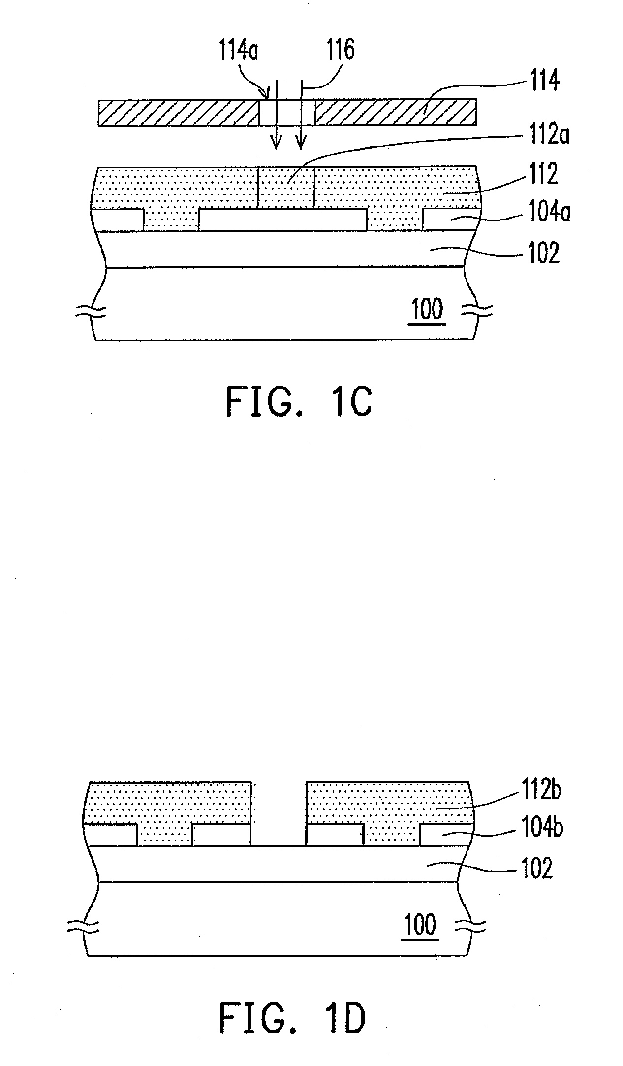
[0025]FIGS. 1A through 1F are cross-sectional views showing a multiple patterning process for patterning a material layer according to one embodiment of the invention. As shown in FIG. 1A, a substrate 100 having a material layer 102 formed thereon is provided. Between the substrate 100 and the material layer 102, there are several inter-layers (not shown). For simplifying the drawings, the inter-layers are not shown in the figures. It should be noticed that the material layer 102 can be, for example but not limited to, formed of polymer, dielectric material, such as silicon oxide or silicon nitride, or other material according to the practical requirement.

[0026]Then, as shown in FIG. 1A, a mask layer 104 is formed on the material layer 102. The mask layer 104 is an anti-reflection mask layer. That is, the mask layer 104 is not only a mask layer for the later performed patterning process of the material layer but also an anti-reflection layer for the later performed photolithography ...


PUM

PropertyMeasurementUnit
temperatureaaaaaaaaaa
optical resolutionaaaaaaaaaa

Abstract

The invention is directed to a method for patterning a material layer. The method comprises steps of forming a mask layer on the material layer. A multiple patterning process is performed on the mask layer for transferring at least a first pattern from a first photomask through a first photoresist and a second pattern from a second photomask from a second photoresist layer into the mask layer without performing any etching process. The mask layer exposes a portion of the material layer and the mask layer is patterned at the time that the first photoresist layer and the second photoresist layer are developed respectively. An etching process is performed to pattern the material layer by using the mask layer as an etching mask.

Description

BACKGROUND OF THE INVENTION[0001]1. Field of Invention[0002]The present invention relates to a patterning process. More particularly, the present invention relates to a multiple patterning process.[0003]2. Description of Related Art[0004]In the manufacture of integrated circuit, photolithography process is used to transfer patterns from a photo mask having customized circuit patterns to thin films formed on a wafer. The image transfer process comprises steps of forming a photoresist layer on a material layer, illuminating the photoresist layer through a photomask having the customized circuit patterns, developing the photoresist layer and then etching the material layer by using the patterned photoresist layer as a mask. Hence, the image transfer process is accomplished. For a well-manufactured integrated circuit product, the image transfer process mentioned above is performed several times to transfer the circuit patterns to each non-process layers to form the electrically circuit ...

Claims


Application Information

Patent Timeline
Patent Type & Authority Applications(United States)
IPC IPC(8): G03C5/00
CPCH01L21/0337H01L21/31144H01L21/0338
Inventor YANG, CHIN-CHENG
Owner MACRONIX INT CO LTD
Why Eureka
Try Eureka