Semiconductor device having two bipolar transistors constituting electrostatic protective element

a technology of bipolar transistors and semiconductors, applied in semiconductor devices, semiconductor/solid-state device details, electrical apparatus, etc., can solve problems such as affecting the internal circuit of objects, and achieve the effect of suppressing the tolerance from lowering and preventing malfunction

Inactive Publication Date: 2009-04-30
RENESAS ELECTRONICS CORP
View PDF2 Cites 6 Cited by
  • Summary
  • Abstract
  • Description
  • Claims
  • Application Information

AI Technical Summary

Benefits of technology

[0026]According to the present invention, therefore, it is possible to provide a semiconductor device capable of supp

Problems solved by technology

In this case, therefore, the malfunction might affect the object in

Method used


Image

  • Semiconductor device having two bipolar transistors constituting electrostatic protective element
  • Semiconductor device having two bipolar transistors constituting electrostatic protective element
  • Semiconductor device having two bipolar transistors constituting electrostatic protective element

Examples


first exemplary embodiment

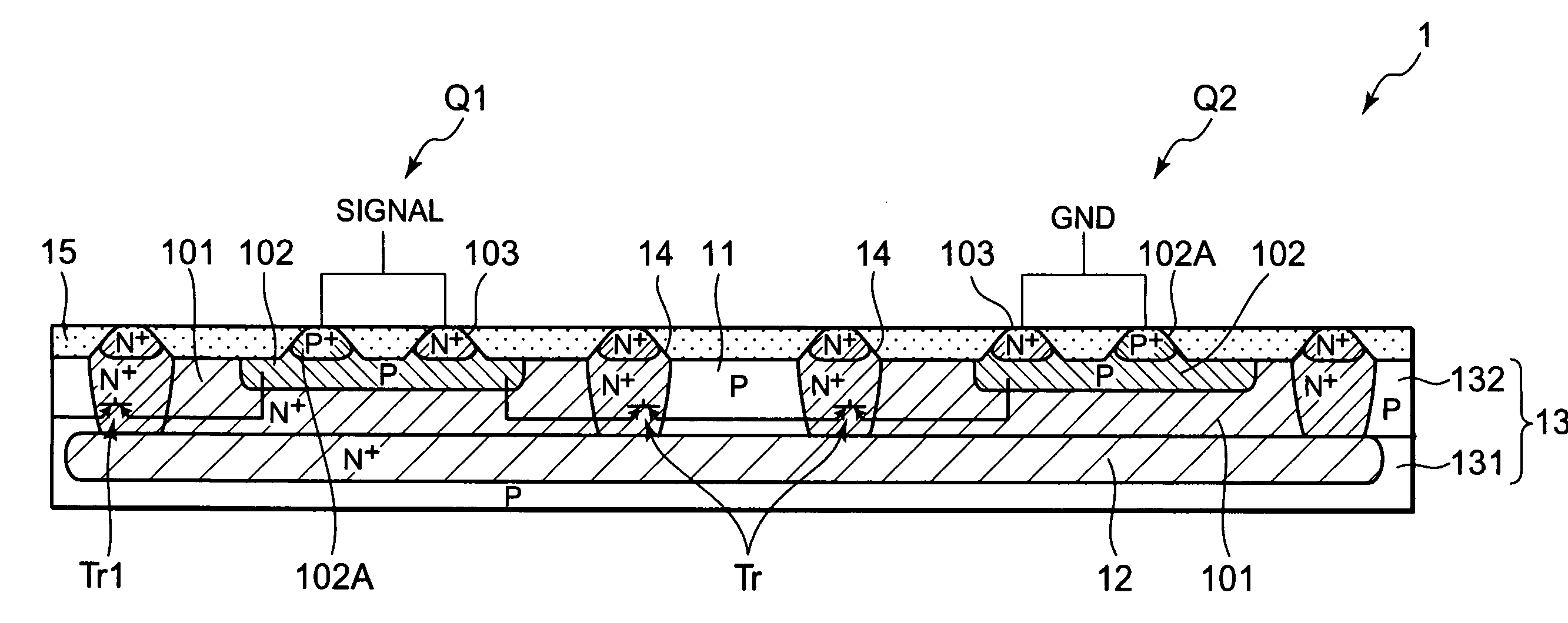
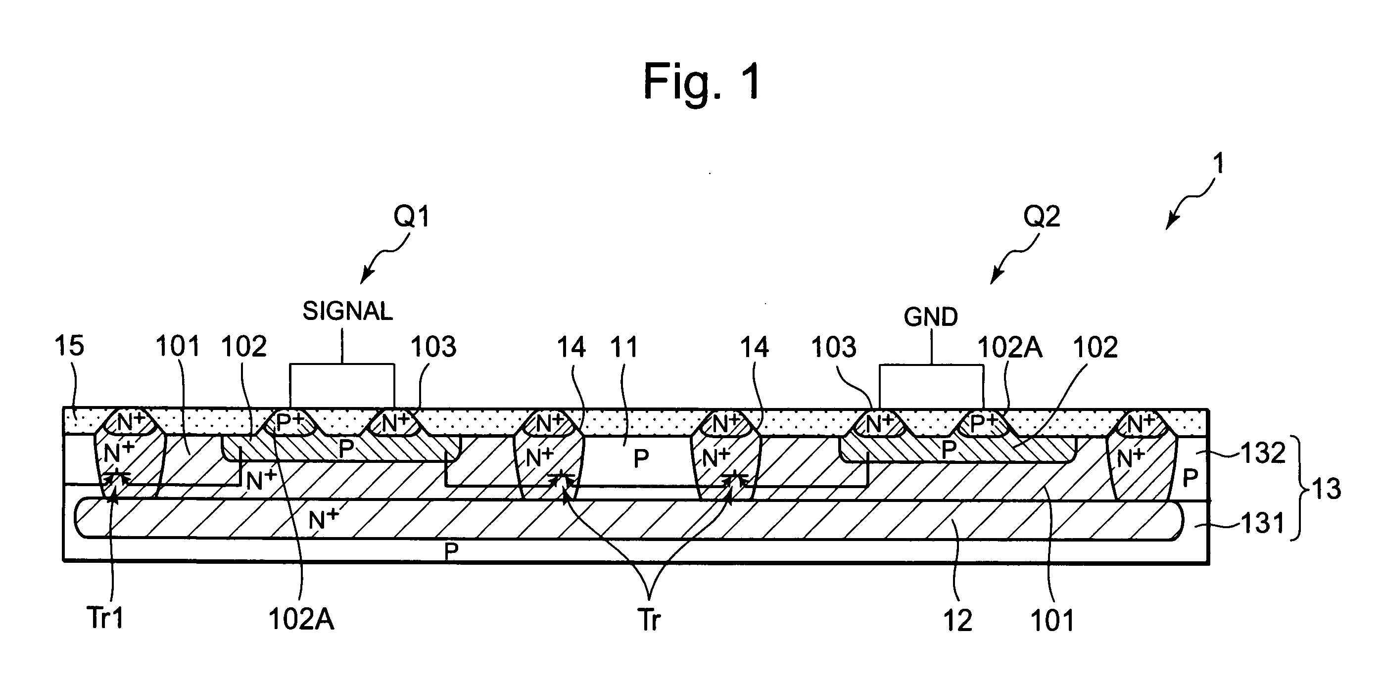
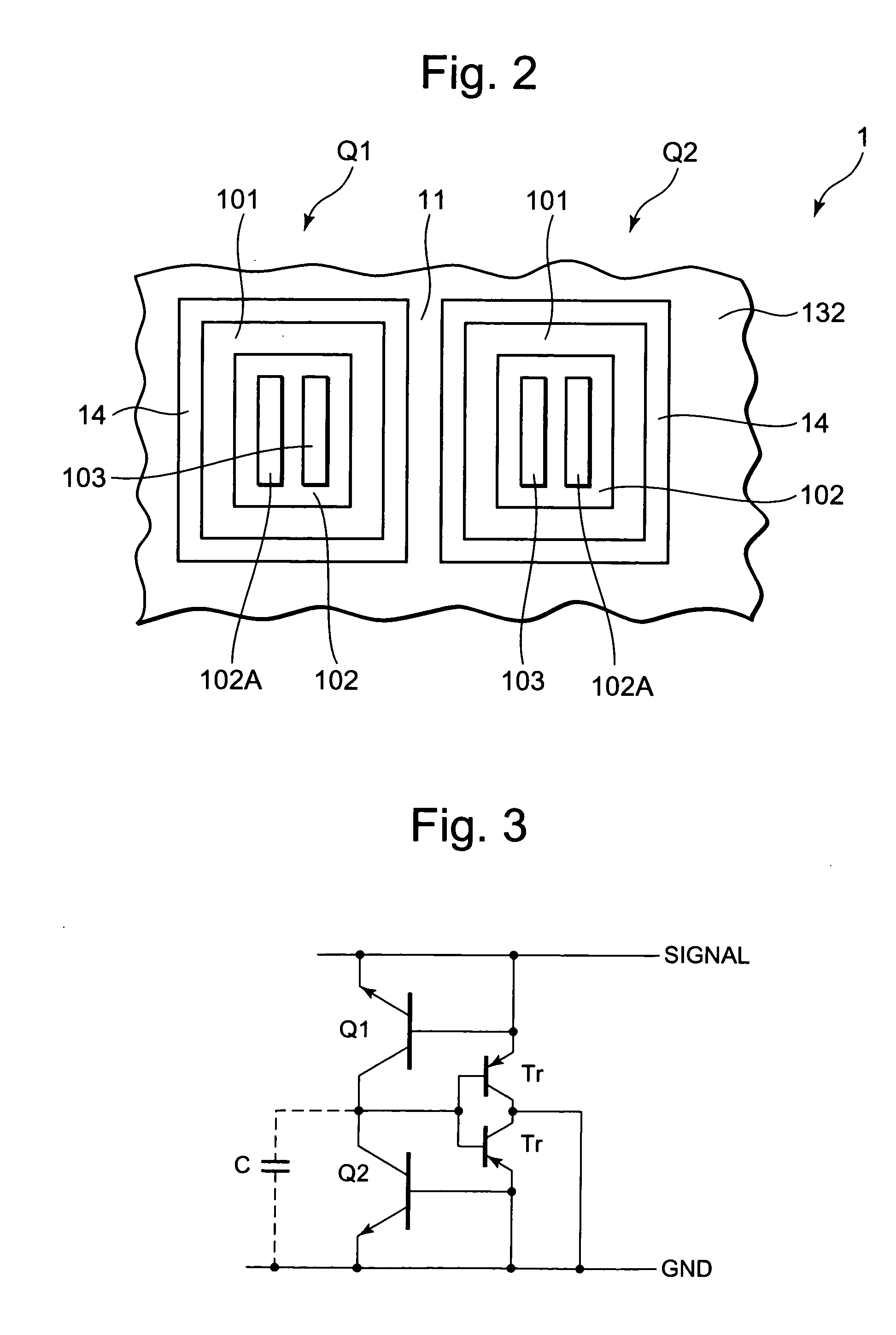
[0038]FIGS. 1 and 2 show a first exemplary embodiment of the present invention.

[0039]The semiconductor device 1 in this first embodiment includes a first conductive type semiconductor substrate 13 having a pair of transistors Q1 and Q2 formed therein.

[0040]Each of the transistors Q1 and Q2 includes a second conductive type collector region 101, a first conductive type base region 102 formed in this collector region 101, and a second conductive type emitter region 103 formed in the base region 102. The first and second conductive types are opposite to each other in conductivity.

[0041]The collector regions of the transistors Q1 and Q2 are disposed separately from each other and a first conductive type first region 11 is formed between those collector regions of the transistors Q1 and Q2.

[0042]The lower portions of the collector regions of the transistors Q1 and Q2 reach a second conductive type buried layer 12 formed in the semiconductor substrate 13 and those collector regions 101 ar...

second exemplary embodiment

[0080]Next, there will be described the second exemplary embodiment of the present invention with reference to FIG. 4.

[0081]In the first exemplary embodiment, the first region 11 is connected to a P type region of the epitaxial layer 132 and configured unitarily with the P type region.

[0082]On the other hand, in case of the semiconductor device 2 in this second exemplary embodiment, as shown in the top view of FIG. 4, the first region 11 is surrounded by the collector pull-out region 14 and the second region 21. Furthermore, the first region 11 is separated from the P type region of the epitaxial layer 132.

[0083]More concretely, the second region 21 is in contact with a portion of the periphery of the first region 11, which is not in contact with the collector pull-out region 14. Concretely, the second region 21 is provided along two sides of the first region 11 that are facing each other.

[0084]This second region 21 is an N+ layer and its bottom reaches the buried layer 12 and is co...


PUM


Abstract

A semiconductor device includes a pair of transistors formed in a first conductive type semiconductor substrate. Each of the transistors contains a collector region of a second conductive type, opposite to the first conductive type, formed in the semiconductor substrate, a base region of the first conductive type formed in the collector region, and an emitter region of the second conductive type formed in the base region, the collector region of one transistor of the pair of transistors being separated from that of the other transistor. The semiconductor device further includes a first region of the first conductive type formed between the collector regions of the pair of transistors, and a buried layer of the second conductive type formed in the semiconductor substrate under the collector region of one transistor of the pair of transistors to connect the collector regions of the transistors therethrough.

Description

BACKGROUND OF THE INVENTION[0001]1. Field of the Invention[0002]The present invention relates to a semiconductor device.[0003]2. Description of Related Art[0004]There has been used a semiconductor device provided with two bipolar transistors as an electrostatic protective element that protects object circuit elements from an overvoltage applied to its terminal.[0005]For example, the patent document 1 (Japanese Unexamined Patent Application Publication No. Hei1(1989)-287954) discloses such a semiconductor device (electrostatic protective element) 400 as shown in FIG. 8.[0006]This semiconductor device 400 has an N type diffusion region 403 as a collector region, as well as two P type diffusion regions 404 and 405 formed in this N type diffusion region 403. The P type diffusion regions 404 and 405 are base regions. In those P type diffusion regions 404 and 405 are formed N type layers 406 and 407 as emitter regions.[0007]In the semiconductor device 400 as described above, if a voltage ...

Claims


Application Information

Patent Timeline
IPC IPC(8): H01L27/082
CPCH01L27/0744H01L27/0262
Inventor SATO, MASAHARU
Owner RENESAS ELECTRONICS CORP
Why Eureka
Try Eureka