Junction structure and method of manufacturing the same
- Summary
- Abstract
- Description
- Claims
- Application Information
AI Technical Summary
Benefits of technology
Problems solved by technology
Method used
Image

Examples
Embodiment Construction
[0019]A junction structure and a method of manufacturing the same according to an embodiment of the present invention will be described below in accordance with the accompanying drawings.
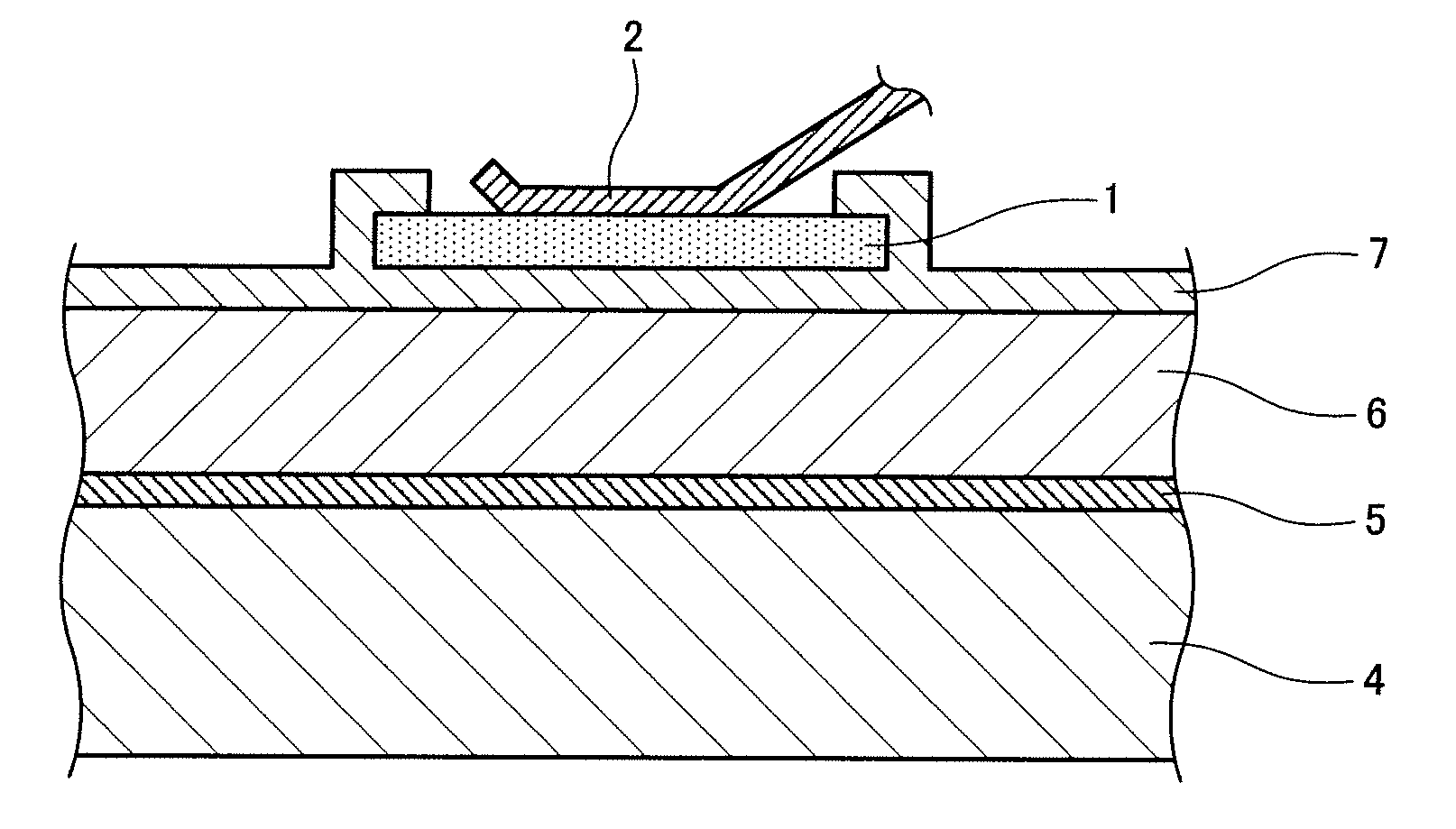
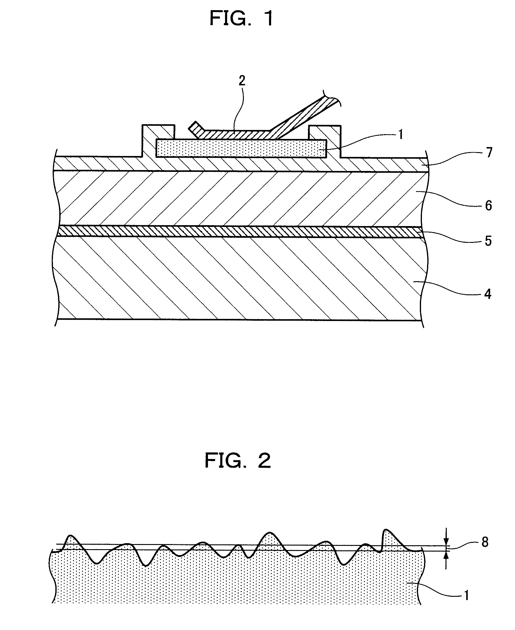
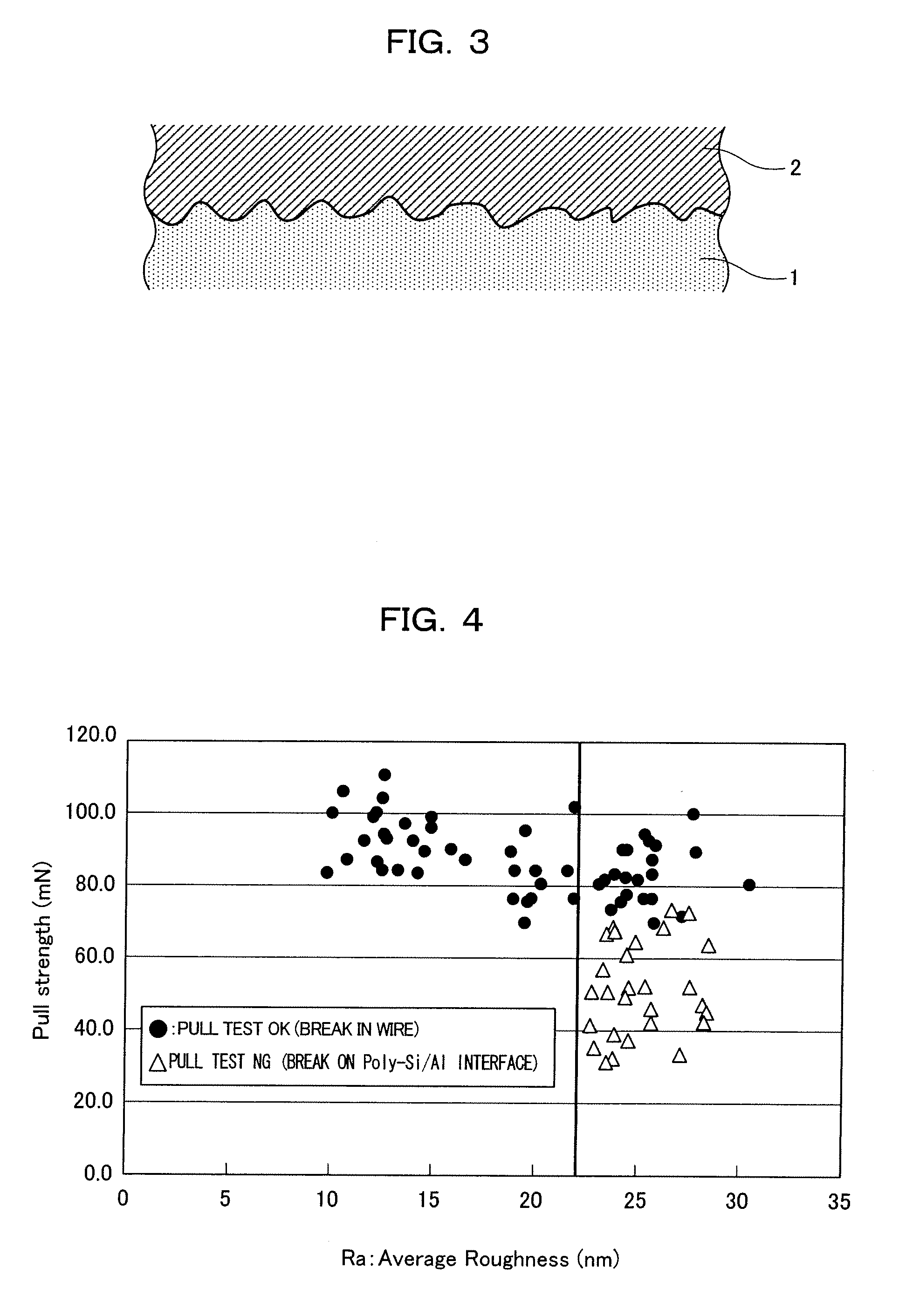
[0020]FIGS. 1 and 2 are a sectional view showing the junction structure according to the embodiment of the present invention, and an enlarged view of the surface of a Poly-Si film bonding pad.
[0021]As shown in FIG. 1, in the junction structure according to the embodiment of the present invention, a SiO2 film 5 is formed on Si 4, a BPSG film 6 is formed on the SiO2 film 5, a SiN film 7 is formed on the BPSG film 6, a Poly-Si film bonding pad 1 is formed on the SiN film 7, and an Al wire 2 is bonded on the Poly-Si film bonding pad 1. In FIG. 2, reference numeral 8 denotes a pad surface average roughness.
[0022]The junction structure is manufactured as follows:
[0023]The SiO2 film 5 is formed on the Si 4 in an atmosphere of oxygen at 1000° C. to 1200° C., and the SiO2 film 5 is reacted by atmospheric pre...
PUM
 Abstract
Description
Claims
Application Information
 - Generate Ideas
- Intellectual Property
- Life Sciences
- Materials
- Tech Scout
- Unparalleled Data Quality
- Higher Quality Content
- 60% Fewer Hallucinations
Browse by: Latest US Patents, China's latest patents, Technical Efficacy Thesaurus, Application Domain, Technology Topic, Popular Technical Reports.
© 2025 PatSnap. All rights reserved.Legal|Privacy policy|Modern Slavery Act Transparency Statement|Sitemap|About US| Contact US: help@patsnap.com