Electro-optical device and electronic apparatus

a technology of optical devices and electronic devices, applied in non-linear optics, instruments, optics, etc., can solve the problems of short wavelengths of selectively reflected light, decrease of contrast, and unsolved following problems, so as to prevent the decrease of contrast due to a temperature change and reduce the driving voltage

Active Publication Date: 2009-04-30
JAPAN DISPLAY WEST
View PDF3 Cites 17 Cited by
  • Summary
  • Abstract
  • Description
  • Claims
  • Application Information

AI Technical Summary

Benefits of technology

[0015]Another aspect of the invention provides an electronic apparatus that includes the above described electro-optical device. In the above aspect of the invention, as in the case of the above described aspects, the driving voltage is lowered, and a decrease in contrast due to a change in temperature is prevented.

Problems solved by technology

In addition, as the amount of additive chiral agent is increased, the wavelengths of selectively reflected light become short.
In the above existing liquid crystal device, however, the following problems remain unsolved.
Furthermore, even when the selectively reflected wavelengths are set to a shorter wavelength side with respect to the visible light range, the selectively reflected wavelengths are shifted into the visible light range because of a change in temperature and, as a result, may decrease the contrast.

Method used


Image

  • Electro-optical device and electronic apparatus
  • Electro-optical device and electronic apparatus
  • Electro-optical device and electronic apparatus

Examples


Embodiment Construction

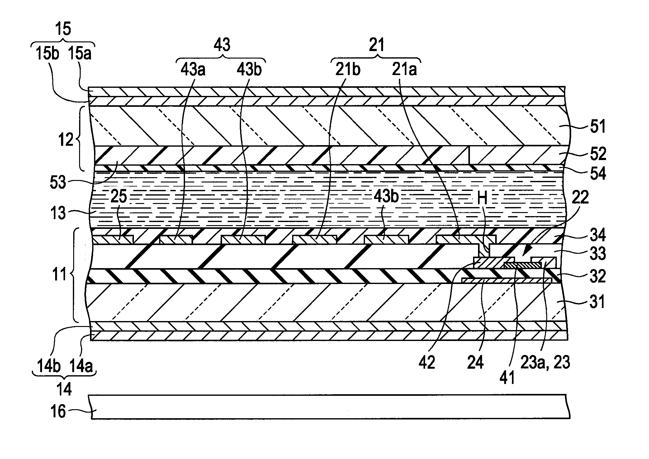
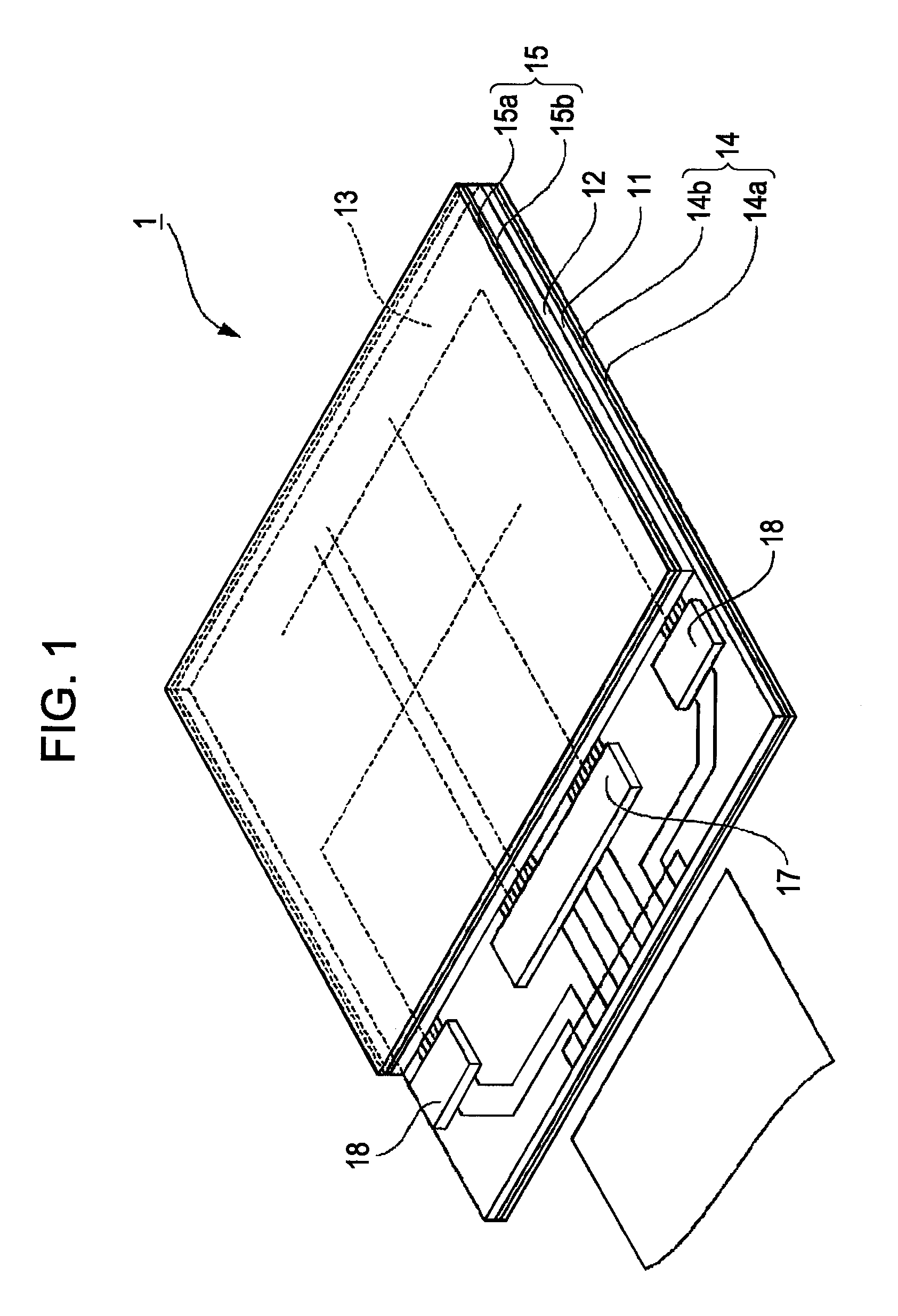
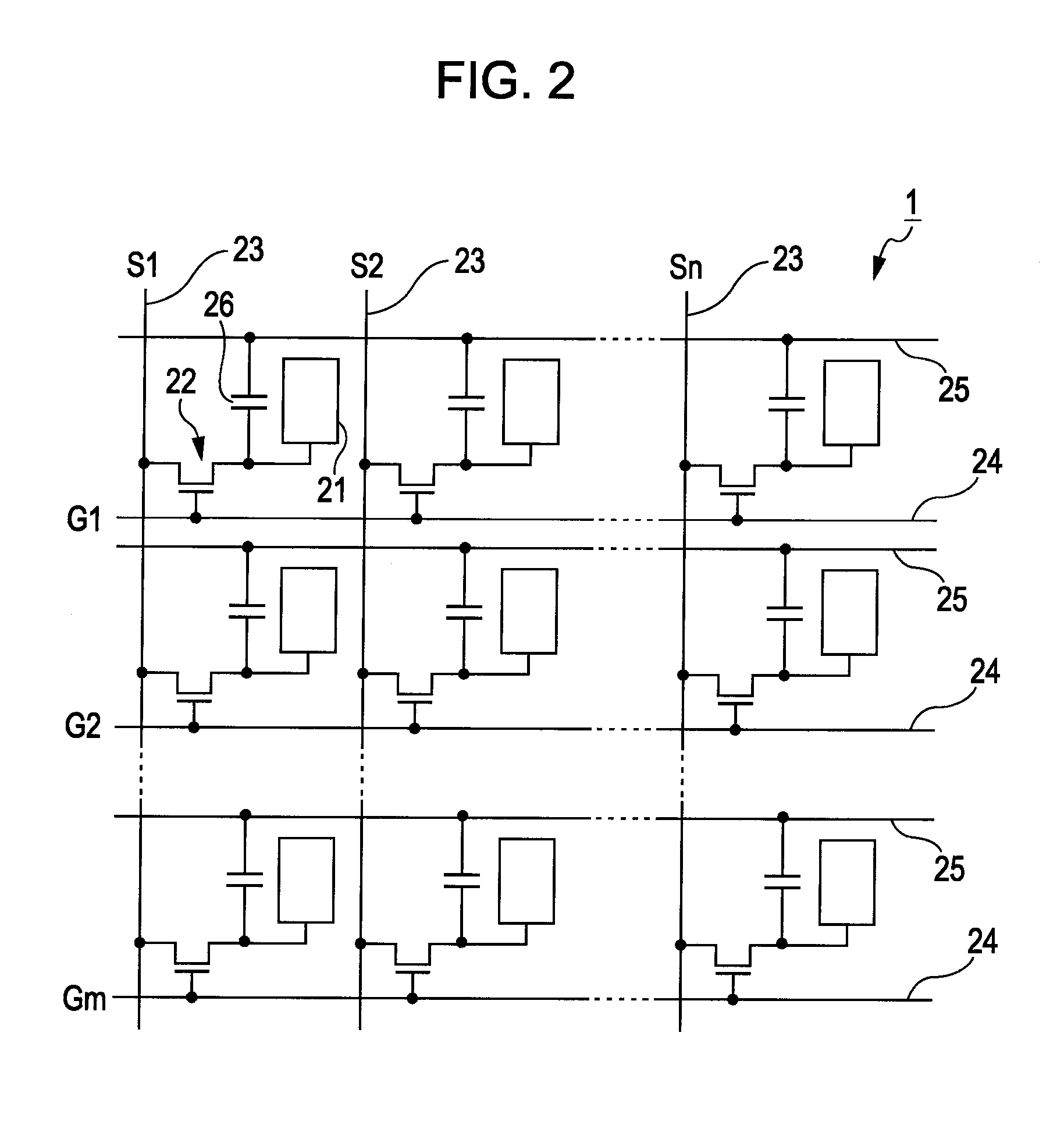
[0022]Hereinafter, an embodiment of a liquid crystal device according to the invention will be described with reference to the accompanying drawings. Note that the scale of the drawings used in the following description is appropriately changed in order to make the components be recognizable. Here, FIG. 1 is a schematic perspective view that shows an electro-optical device. FIG. 2 is an equivalent circuit diagram of FIG. 1. FIG. 3A is a plan view that shows a pixel area. FIG. 3B is a cross-sectional view taken along the line IIIB-IIIB in FIG. 3A.

Liquid Crystal Device

[0023]The liquid crystal device (electro-optical device) 1 according to the present embodiment, as shown in FIG. 1, includes, an element substrate (first substrate) 11, an opposite substrate (second substrate) 12, and a liquid crystal layer 13 that is held between the element substrate 11 and the opposite substrate 12. In addition, the liquid crystal device 1 is formed so that the element substrate 11 and the opposite su...


PUM

PropertyMeasurementUnit
peak wavelengthaaaaaaaaaa
optical isotropyaaaaaaaaaa
optical anisotropyaaaaaaaaaa

Abstract

An electro-optical device includes, a first substrate, a second substrate, an electrooptic material layer, an illuminating device, and a polarizing device. The electrooptic material layer is held between the first substrate and the second substrate. The illuminating device irradiates illumination light to an outer surface of the first substrate. The polarizing device is provided on the outer surface of the first substrate. The electrooptic material layer exhibits optical isotropy when no electric field is applied, and, when an electric field is applied, exhibits optical anisotropy corresponding to the magnitude of the electric field. The electrooptic material layer further has a characteristic to selectively reflect a first circularly polarized light having a first rotation direction. Light that passes through the polarizing device is a second circularly polarized light that has a second rotation direction reverse to the first rotation direction of the first circularly polarized light.

Description

BACKGROUND[0001]1. Technical Field[0002]The present invention relates to an electro-optical device and an electronic apparatus.[0003]2. Related Art[0004]An electro-optical device that uses electronic polarization due to Kerr effect is known. The Kerr effect is a phenomenon that, when an electric field is applied, exhibits optical anisotropy which has an axis in the direction of the electric field and of which the degree is proportional to the square of the magnitude of the electric field. A known electrooptic material that exhibits the above Kerr effect is a liquid crystal material called a blue phase, for example. It has been known that a liquid crystal device (see JP-A-2000-275605) that employs a blue phase as a liquid crystal layer has a quick response speed. The blue phase exhibits optical isotropy when no electric field is applied, and exhibits optical anisotropy that is proportional to the square of the magnitude of an electric field applied under a predetermined temperature r...

Claims


Application Information

Patent Timeline
Patent Type & Authority Applications(United States)
IPC IPC(8): G02F1/1335
CPCG02F1/13718G02F1/134363
Inventor HARUYAMA, AKIHIDE
Owner JAPAN DISPLAY WEST
Why Eureka
Try Eureka