Low current switching magnetic tunnel junction design for magnetic memory using domain wall motion
Active Publication Date: 2009-04-30
AVALANCHE TECH
View PDF38 Cites 37 Cited by
Summary
Abstract
Description
Claims
Application Information
AI Technical Summary
This helps you quickly interpret patents by identifying the three key elements:
Problems solved by technology
Method used
Benefits of technology
[0012]Briefly, a multi-state low-current-switching magnetic memory element (magnetic memory element) using domain wall positioning to define the memory state is disclosed. The magnetic memory element comprises a substantially flat, elongated free layer, with stacks disposed on each end. The stacks serve both as electrodes, and, due to each having a unique magnetic moment, pin each end of the free layer in opposite magnetic directions. The pinned magnetic moments generate a well-defined domain wall within the free layer. Disposed central t
Problems solved by technology
Though widely used and commonly accepted, such hard disk drives suffer from a variety of deficiencies.
Access latency, higher power dissipation, increased physical size and inability to withstand any physical shock justifies a new type of storage device.
Other dominant semiconductor based storage devices are DRAM and SRAM which are volatile and very costly, but have faster random read/write time.
Although NAND flash memory is more costly, it has replaced HDDs in many applications such as digital cameras, MP3 players, cell phones, and hand held multimedia devices.
However, as process geometry is getting smaller, the design of NAND flash memory and DRAM memory is becoming more difficult to scale.
For example, NAND flash memory has issues related to capacitive coupling, few electrons/bit, poor error-rate performance, and poor reliability due to low read-write endurance.
It is believed that NAND flash memory, especially multi-bit designs will be extremely difficult to scale be
Method used
Image
Click on the blue label to locate the original text in one second.
Reading with bidirectional positioning of images and text.
Examples
Embodiment Construction
[0027]In the following description of the embodiments, reference is made to the accompanying drawings that form a part hereof, and in which is shown by way of illustration of the specific embodiments in which the invention may be practiced. It is to be understood that other embodiments may be utilized because structural changes may be made without departing from the scope of the present invention. It should be noted that the figures discussed herein are not drawn to scale and thicknesses of lines are not indicative of actual sizes.
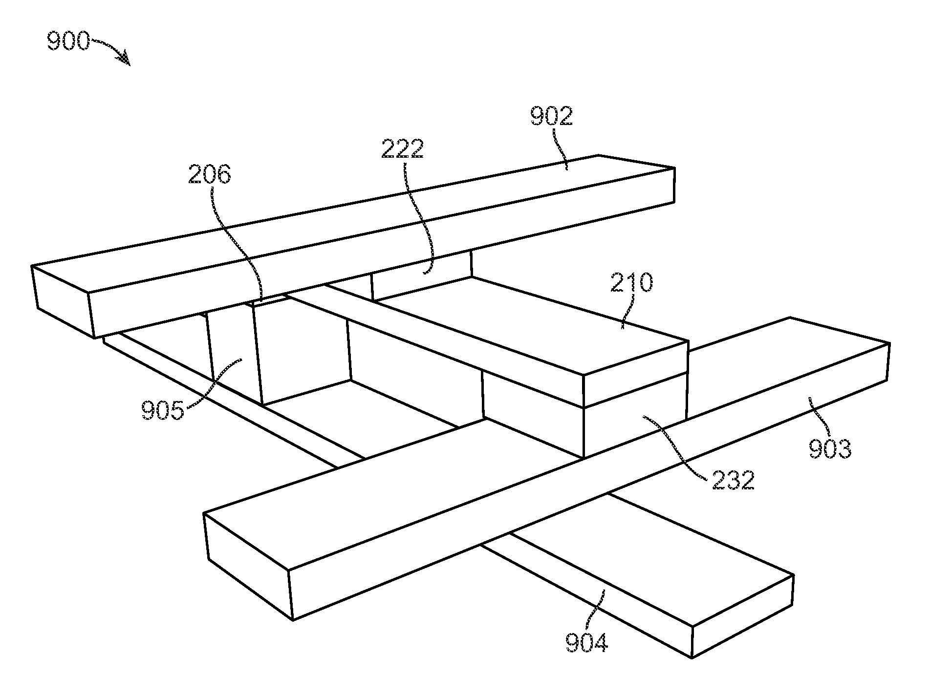
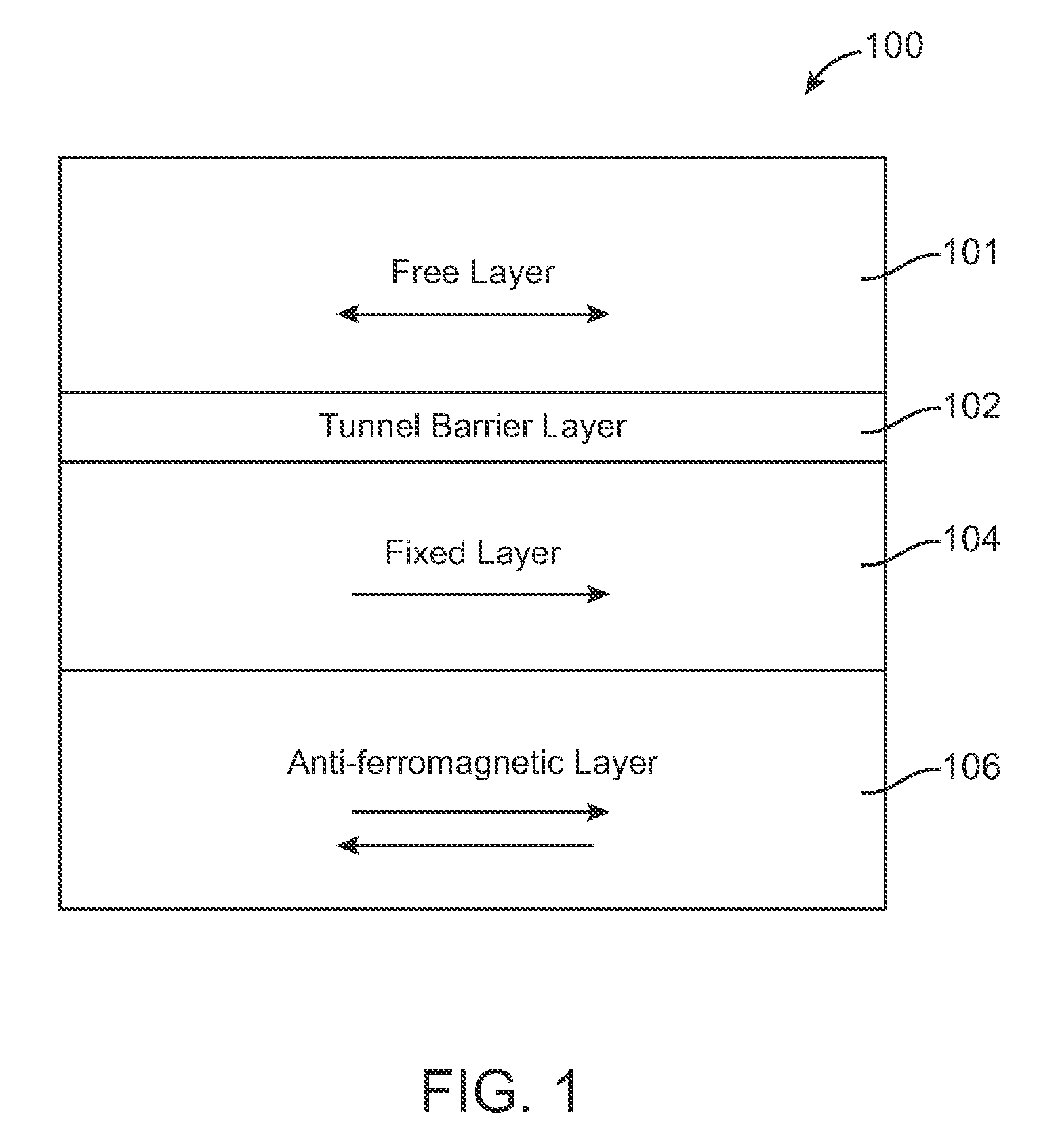
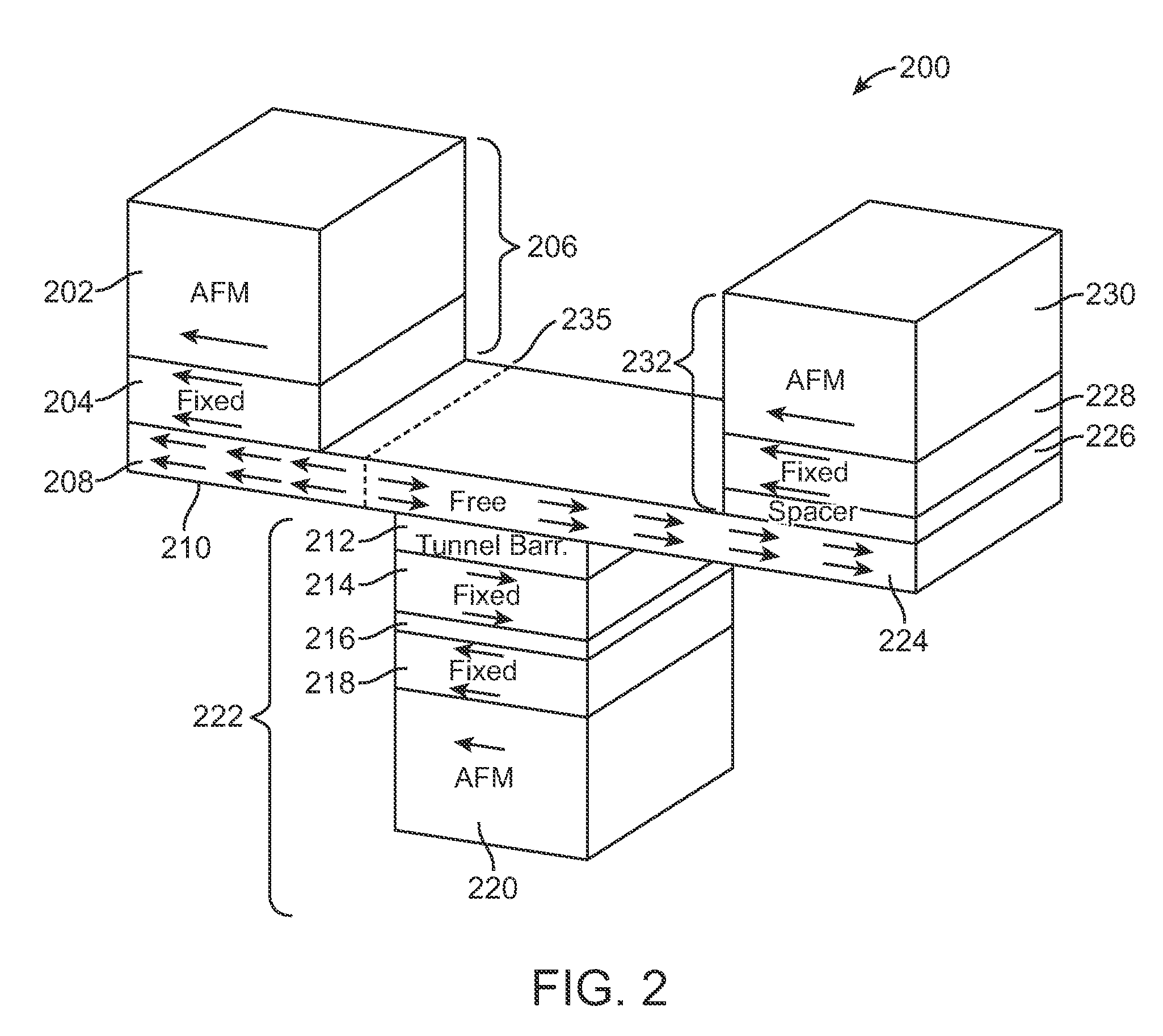
[0028]In an embodiment of the present invention a magnetic tunnel junction (MTJ) is located central to a free layer, with the free layer having stacks with pinned magnetic moments on either end, and the end-defining stacks creating a well defined magnetic domain state of the free layer therebetween. Pushing the free layer's domain wall towards either stack modifies the domain state of the free layer. The domain wall is pushed by the passage of electron cur...
PUM
Abstract
A multi-state low-current-switching magnetic memory element (magnetic memory element) comprising a free layer, two stacks, and a magnetic tunneling junction is disclosed. The stacks and magnetic tunneling junction are disposed upon surfaces of the free layer, with the magnetic tunneling junction located between the stacks. The stacks pin magnetic domains within the free layer, creating a free layer domain wall. A current passed from stack to stack pushes the domain wall, repositioning the domain wall within the free layer. The position of the domain wall relative to the magnetic tunnel junction corresponds to a unique resistance value, and passing current from a stack to the magnetic tunnel junction reads the magnetic memory element's resistance. Thus, unique memory states may be achieved by moving the domain wall.
Description
CROSS REFERENCE TO RELATED APPLICATIONS[0001]This application claims benefit of U.S. Provisional Patent Application, entitled “Low Current Switching Magnetic Tunnel Junction Design for Magnetic Memory using Domain Wall Motion,” U.S. Provisional Application No. 61 / 001,348, filed on Oct. 31, 2007, and from U.S. patent application Ser. No. 11 / 674,124, entitled “Non-Uniform Switching Based Non-Volatile Magnetic Base Memory,” filed Feb. 12, 2007, by Ranjan, et al., U.S. patent application Ser. No. 11 / 678,515, entitled “A High Capacity Low Cost Multi-State Magnetic Memory,” filed Aug. 23, 2008, by Ranjan, et al., U.S. patent application Ser. No. 11 / 776,692, entitled “Non-Volatile Magnetic Memory Element with Graded Layer,” filed Jul. 12, 2007, by Ranjan, et al., U.S. patent application Ser. No. 11 / 740,861, entitled “High Capacity Low Cost Multi-Stacked Cross-Line Magnetic Memory,” filed Apr. 26, 2007, by Ranjan, et al., and U.S. Provisional Patent Application No. 61 / 045,582, entitled “Low...
Claims
Application Information
Patent Timeline
Application Date:The date an application was filed.
Publication Date:The date a patent or application was officially published.
First Publication Date:The earliest publication date of a patent with the same application number.
Issue Date:Publication date of the patent grant document.
PCT Entry Date:The Entry date of PCT National Phase.
Estimated Expiry Date:The statutory expiry date of a patent right according to the Patent Law, and it is the longest term of protection that the patent right can achieve without the termination of the patent right due to other reasons(Term extension factor has been taken into account ).
Invalid Date:Actual expiry date is based on effective date or publication date of legal transaction data of invalid patent.