

Microchip and Method of Using the Same
a microchip and chip technology, applied in the field of microchips, can solve the problems of decreasing the merits of using the microchip, and achieve the effects of accurate alignment, facilitating the alignment of the optical axis, and increasing the cross-sectional area of the optical measurement cuv
- Summary
- Abstract
- Description
- Claims
- Application Information
AI Technical Summary
Benefits of technology
Problems solved by technology
Method used
Image

Examples
first embodiment
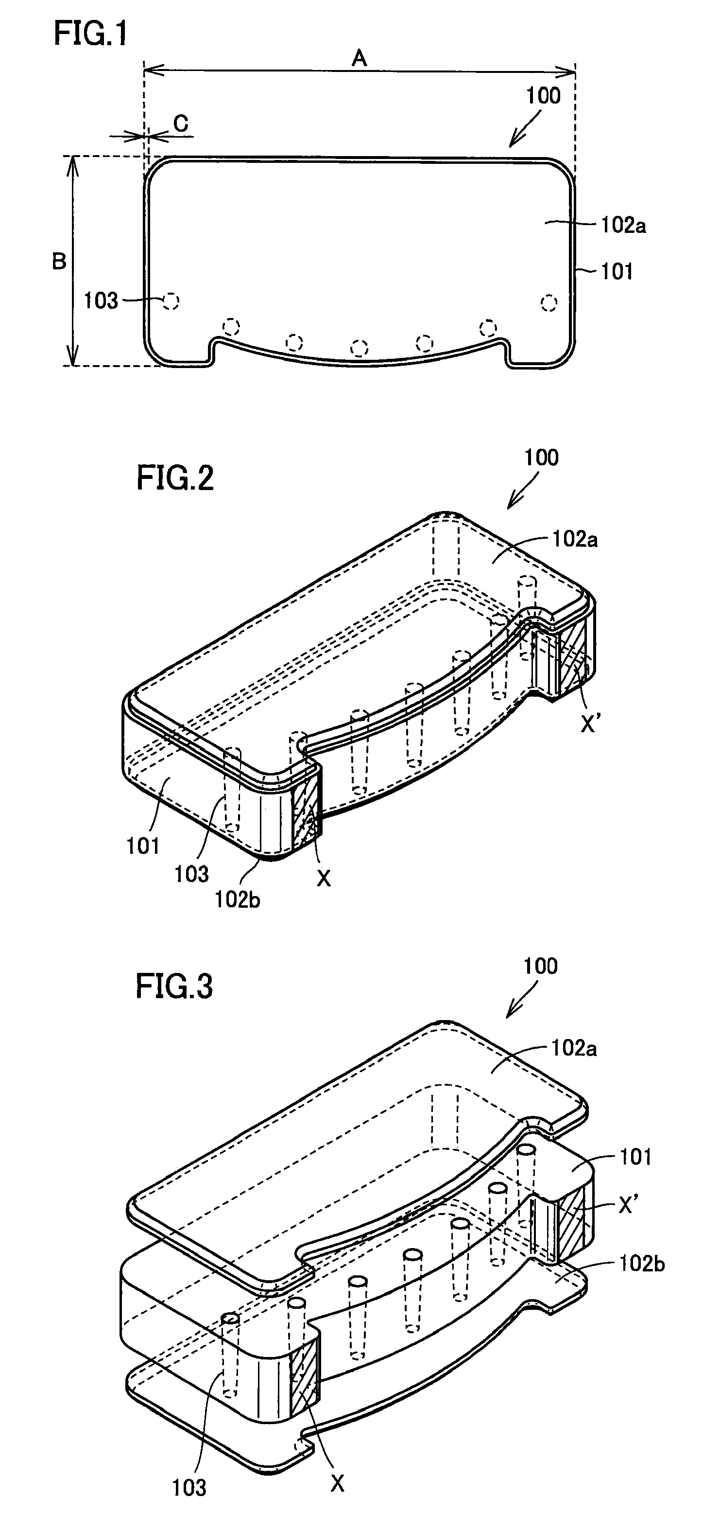
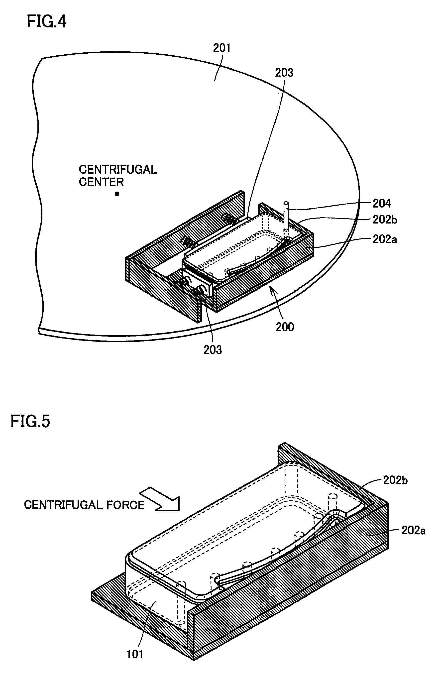
[0057]FIGS. 1 to 3 are schematic views showing one example of a microchip according to a first embodiment of the present invention, where FIG. 1 is a schematic top view, FIG. 2 is a schematic perspective view, and FIG. 3 is a schematic exploded perspective view. A microchip 100 shown in FIGS. 1 to 3 is configured by laminating a first substrate 101, and two second substrates 102a and 102b which are transparent substrates, in such manner that second substrates 102a and 102b sandwich first substrate 101. First substrate 101 is formed with a total of seven pass-through holes 103 passing in a thickness direction of the substrate, and substrate surfaces of two second substrates 102a and 102b seal an opening of pass-through hole 103. A diameter of the opening of pass-through hole 103 on second substrate 102b side is about 1 mm, and a diameter of the opening on second substrate 102a side is about 1.5 mm. Such opening diameters are not particularly limited. A space (cavity) configured by pa...
second embodiment
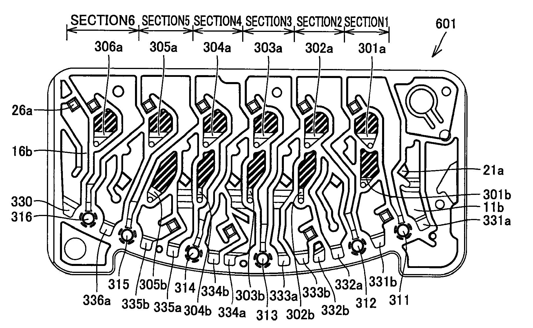
[0084]A microchip according to a second embodiment of the present invention will now be described. FIGS. 10A to 10C are schematic views showing one example of the microchip according to the second embodiment of the present invention, where FIG. 10A is a schematic top view, FIG. 10B is a schematic side view, and FIG. 10C is a schematic bottom view. A microchip 600 shown in FIGS. 10A to 10C is formed by laminating two second substrates 602, 603 that are transparent substrates, on both sides of a first substrate 601 that is a black substrate (see FIG. 10B). Vertical and horizontal lengths of the substrates are not particularly limited, and may be about 62 mm horizontally (A′ in FIG. 10A)×about 30 mm vertically (B′ in FIG. 10A). Thicknesses of second substrate 602, first substrate 601, and second substrate 603 (C′, D′, and E′ in FIG. 10B) may be, for example about 1.6 mm, about 9 mm′ and about 1.6 mm, respectively. The vertical and horizontal lengths and the thickness of the substrate a...
third embodiment
[0121]FIG. 21 is a schematic perspective view showing one example of an outer shape of a microchip according to a third embodiment of the present invention. A microchip 900 shown in FIG. 21 is formed by laminating two substrates of a first substrate 901 and a second substrate 902, and has a substantially flat plate shape. An optical measurement cuvette (detecting portion) for analyzing and / or examining the mixed liquid of the specimen and the liquid reagent etc., which is one part of the fluid circuit formed in the microchip is formed in a projection 903. One corner of the corners at the outer edge of microchip 900 has a cutout 904.
[0122]The microchip no longer has a symmetry plane and a symmetry center by forming cutout 904 at the outer edge of the microchip, and thus the microchip can be fitted in the correct orientation without mistaking the orientation when being fitted to the centrifugal device. Further, in manufacturing the microchip, first substrate 901 and second substrate 9...
PUM
| Property | Measurement | Unit |
|---|---|---|
| Fraction | aaaaa | aaaaa |
| Time | aaaaa | aaaaa |
| Thickness | aaaaa | aaaaa |
Abstract
Description
Claims
Application Information