Semiconductor device

a semiconductor device and semiconductor technology, applied in the direction of semiconductor devices, electrical devices, transistors, etc., can solve the problems of adverse influence, adverse influence of device properties, adverse influence of device residual stress, etc., and achieve uniform and high stability of semiconductor devices and improve yield

Inactive Publication Date: 2009-05-07
CANON KK
View PDF6 Cites 3984 Cited by
  • Summary
  • Abstract
  • Description
  • Claims
  • Application Information

AI Technical Summary

Benefits of technology

[0013]According to the present invention, an adverse effect caused by thermal shrinkage or thermal expansion can be avoided. As a result

Problems solved by technology

When a flexible substrate such as a plastic plate or a resin film is used, factors with respect to warpage of a thin film lamination including the substrate, change in size which is caused by, for example, thermal shrinkage or thermal expansion, and residual stress are adversely influenced for the device on it.
In particular, when a plastic film obtained by melt-processing a thermoplastic r

Method used


Image

  • Semiconductor device
  • Semiconductor device
  • Semiconductor device

Examples


example 1

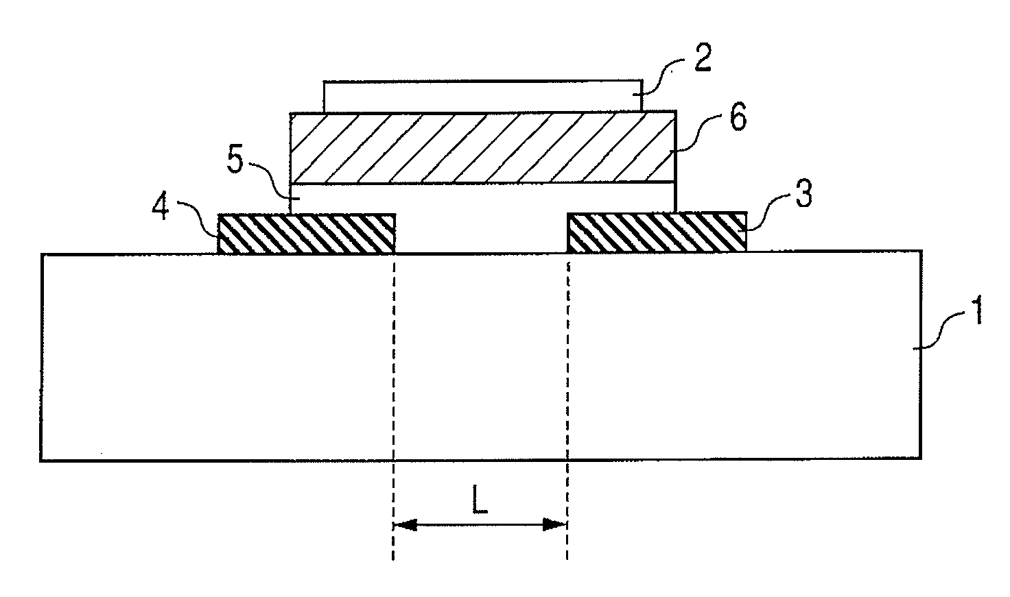
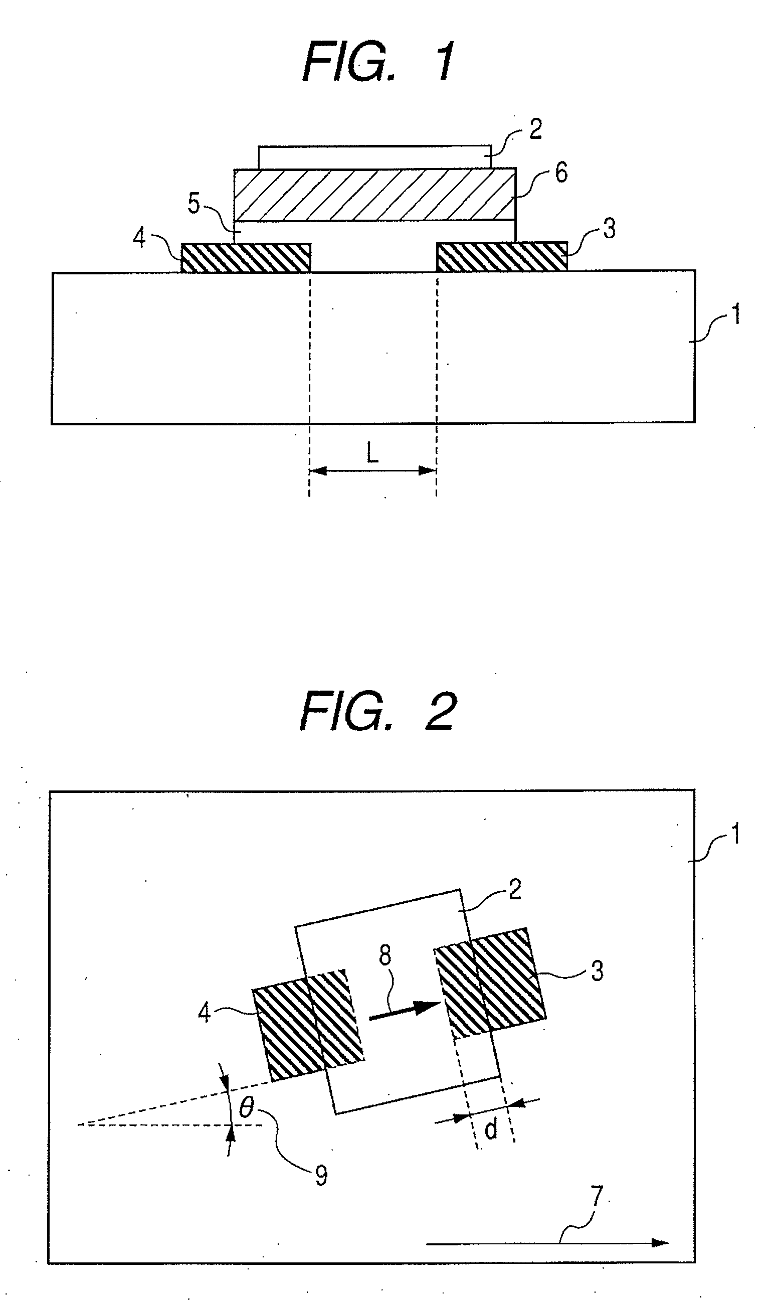
[0060]An example of fabrication of a TFT using an amorphous In—Ga—Zn—O thin film for a channel is shown in which the channel is formed on a biaxially stretched plastic film substrate such that the direction of a current flowing in the channel of the TFT is nonparallel to the direction in which thermal shrinkage rate of the plastic film substrate is largest. The TFT manufactured on the plastic film substrate is a top gate TFT device and has the same structure as that which is described earlier and shown in FIGS. 1 and 2.

[0061]The plastic film substrate to be used is a sheet-like plastic film (biaxially stretched polyethylene terephthalate film produced by TORAY Industries, Inc., whose product name is Lumira, product number is T56, thickness is 125 microns, size is 5 cm square, longitudinal (film longitudinal) thermal shrinkage rate is 1.2, andtransverse thermal shrinkage rate is 0.5).

[0062]As shown in FIG. 2, a drain electrode and a source electrode is patterned on a film surface by ...

example 2

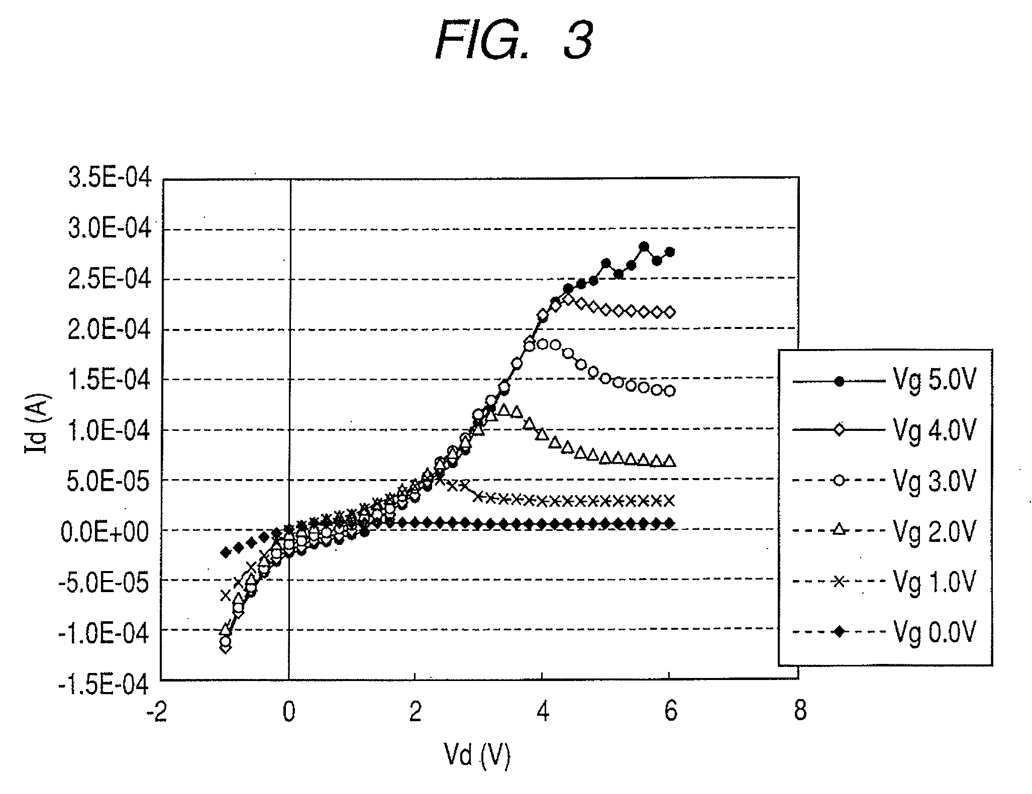
[0067]A TFT device having the same size as that in Example 1 is manufactured and the angle θ is set to 45°. FIG. 5 shows a current (IDS) to voltage (VDS) characteristic of the TFT device (whose channel length is 3 micron, channel width is 30 micron, and angle θ is 45°) which was measured at room temperature. FIG. 6 shows a current (IDS) to voltage (VGS) characteristic of the TFT device which was measured at the room temperature. The threshold value of the gate voltage VGS at VDS=6 V was approximately 0.64 V. At VGS=6 V, the current IDS=1.83×10⁻⁴ A flowed. The S-value of the sub-threshold slope characteristics was approximately 0.14 V / dec. The field-effect mobility was calculated from the output characteristics. As a result, the field-effect mobility was found to be approximately 17.1 cm2 (V·sec.)−1 in the saturation region.


PUM


Abstract

In the present invention, a thin film transistor is formed on a plastic film substrate (1) having anisotropy of thermal shrinkage rate or coefficient of thermal expansion in in-plane directions of the substrate. A channel is formed such thatthe direction (7) in which the thermal shrinkage rate or the coefficient of thermal expansion of the substrate is largest is nonparallel tothe direction (8) of a current flowing through the channel of the thin film transistor. Then, a thin film transistor having stable and uniform electrical characteristics, which is formed on the plastic film substrate, is provided.

Description

TECHNICAL FIELD[0001]The present invention relates to a semiconductor device formed on a substrate having anisotropy of thermal shrinkage rate or coefficient of thermal expansion in in-plane directions of the substrate.BACKGROUND ART[0002]In recent years, light-emitting devices, display panels, and the like which are placed on a substrate which is flexible and light-weight have been under active research and development. For example, a thin film transistor (TFT) in which a transparent conductive oxide polycrystalline thin film containing ZnO as main material is used as a channel layer has been actively developed (see Japanese Patent Application Laid-Open No. 2002-76356).[0003]The thin film can be formed at low temperature and is transparent to visible light, so it makes possible a flexible transparent TFT to be formed on a substrate such as a plastic plate or a film.[0004]On the other hand, a thin film formed on a film-shaped flexible substrate by a vapor phase method has been a pro...

Claims


Application Information

Patent Timeline
IPC IPC(8): H01L29/786
CPCH01L27/1296H01L29/7869H01L29/78603H01L27/1218
Inventor CHANG, CHIENLIU
Owner CANON KK
Why Eureka
Try Eureka