Resin-sealed light emitting device and its manufacturing method

a technology of resin-sealed light and light-emitting device, which is applied in the direction of solid-state devices, optical articles, other domestic articles, etc., can solve the problems of insufficient heat radiation characteristics of led packages, increased production costs, and increased production costs, and achieves high reliability and long life. , the effect of high heat radiation characteristics

Inactive Publication Date: 2009-05-07
TOWA
View PDF6 Cites 52 Cited by
  • Summary
  • Abstract
  • Description
  • Claims
  • Application Information

AI Technical Summary

Benefits of technology

[0022]According to the present invention, setting pattern (5) on which LED chip (3) is set, and heat radiating pattern (7) to radiate the heat generated in LED chip (3) outside resin-sealed light emitting device (1A, 1B, 14, 19, 21, 23, 25) are provided, and setting pattern (5) and heat radiating pattern (7) are connected. Thus, the heat generated in LED chip (3) can be radiated effectively outside resin-sealed light emitting device (1A, 1B, 14, 19, 21, 23, 25) through setting pattern (5) and heat radiating pattern (7) sequentially. Thus, the heat radiation characteristics of resin-sealed light emitting device (1A, 1B, 14, 19, 21, 23, 25) is improved. Therefore, the high reliability and long life of resin-sealed light emitting device (1A, 1B, 14, 19, 21, 23, 25) can be implemented.
[0023]In addition, according to the present invention, recessed part (26) is provided in each of one or more regions (16) in the one surface of circuit substrate (15), and light reflection part (10) is provided on slanted surface (9) of recessed part (26). Thus, one part of the light emitted from LED chip (3) is efficiently reflected by light reflection part (10) and emitted upward, for example. Therefore, in addition to the above effect, the luminance efficiency of resin-sealed light emitting device (1A, 1B, 14, 19, 21, 23, 25) is improved.
[0024]Furthermore, according to one example of the present invention, recessed part (26) is provided in each of plurality of region (16) in the one surface of circuit substrate (15), and one or more LED chips (3) mounted on each recessed part (26) are sealed all at once in entire circuit substrate (15). Thus, resin-sealed light emitting device (1A, 1B, 14, 19, 21, 23, 25) is produced by separating the sealed body into individual bodies by one or more regions (16) as needed. Therefore, in addition to the above effect, resin-sealed light emitting device (1A, 1B, 14, 19, 21, 23, 25) can be efficiently produced.

Problems solved by technology

However, according to the above conventional technique, the problem is that heat radiation characteristics as the LED package is not sufficient.
Especially, when a printed substrate formed of a glass epoxy substrate is used as the substrate, this problem is evident.
In addition, this problem becomes more evident as an output of the LED package becomes high recently (increase in light flux per LED package).

Method used


Image

  • Resin-sealed light emitting device and its manufacturing method
  • Resin-sealed light emitting device and its manufacturing method
  • Resin-sealed light emitting device and its manufacturing method

Examples


first embodiment

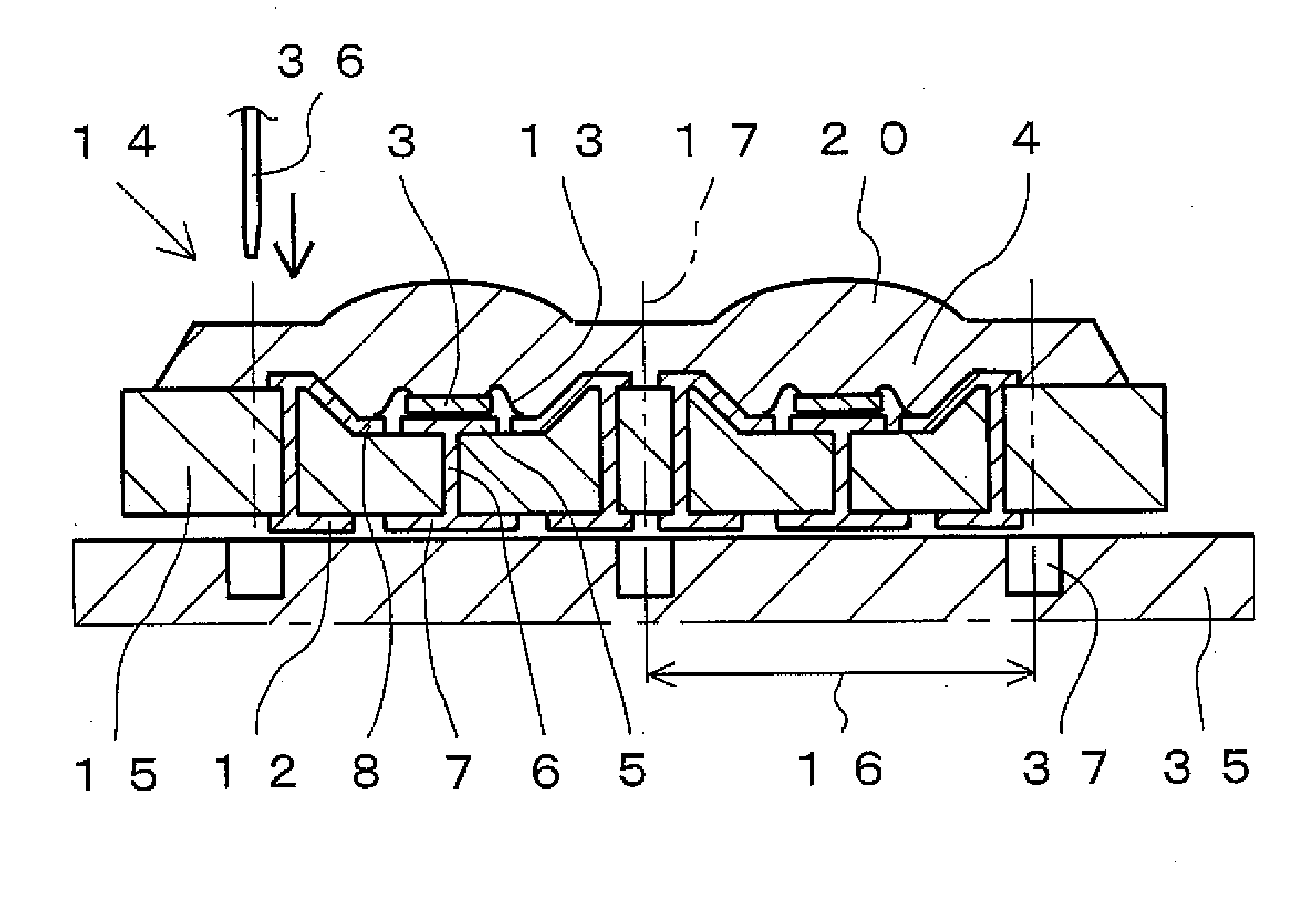
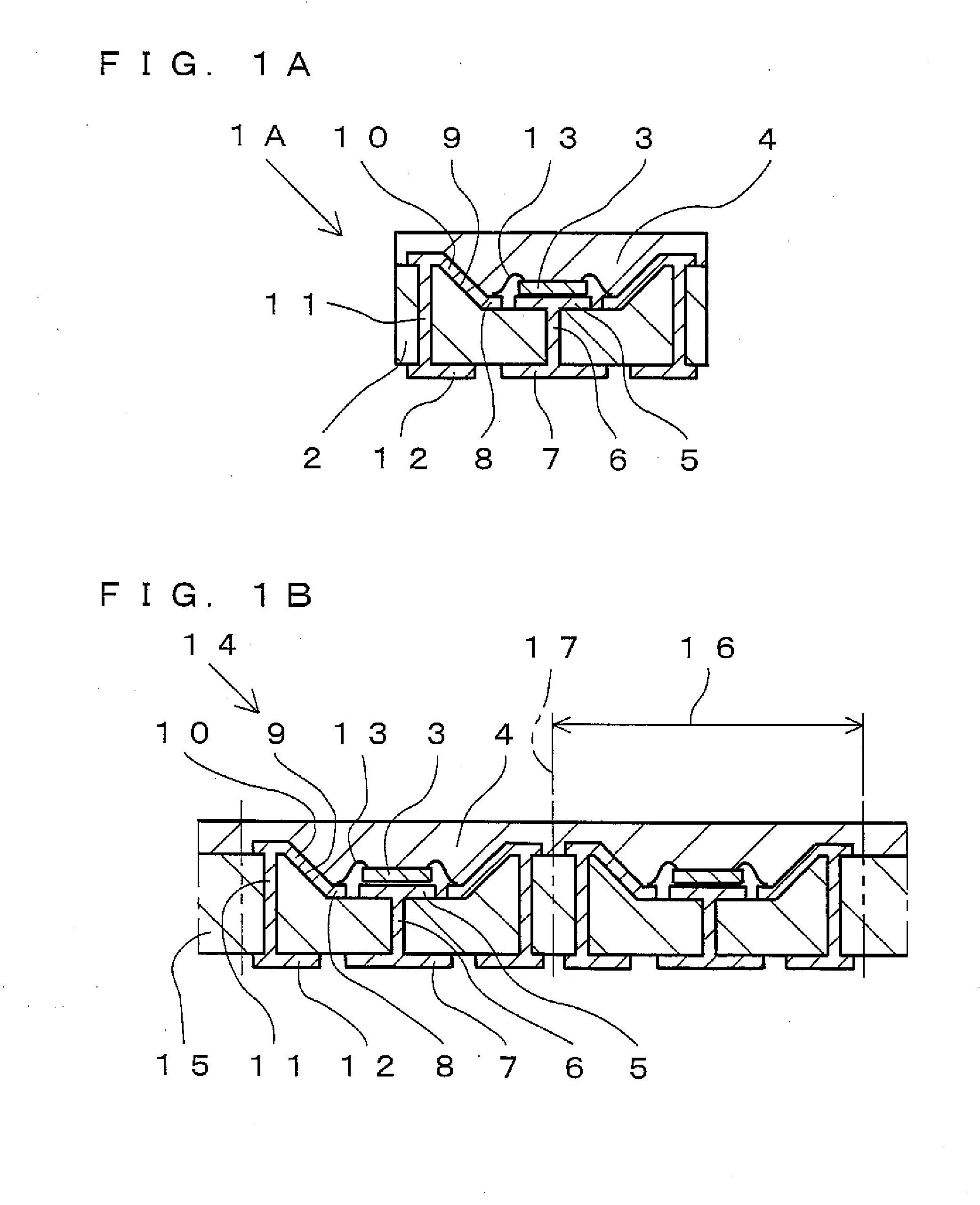
[0039]With reference to FIGS. 1A and 1B, a first embodiment regarding a resin-sealed light emitting device according to the present invention will be described. FIGS. 1A and 1B are front vertical sectional views showing a resin-sealed light emitting device according to this embodiment and a sealed body as an intermediate body in a production process of the resin-sealed light emitting device shown in FIG. 1A, respectively. Note that components are exaggerated or simplified in the drawings used in the following description so as to be easily understood. In addition, the same reference numeral is allotted to the same component in each drawing.

[0040]First, LED package 1A as the resin-sealed light emitting device shown in FIG. 1A will be described. The main components in LED package A are substrate 2, LED chip 3 mounted in the recessed part (see a recessed part 26 in FIG. 7A) provided in one surface (an upper surface in the drawing) of substrate 2, and a translucent sealing resin 4. Sett...

second embodiment

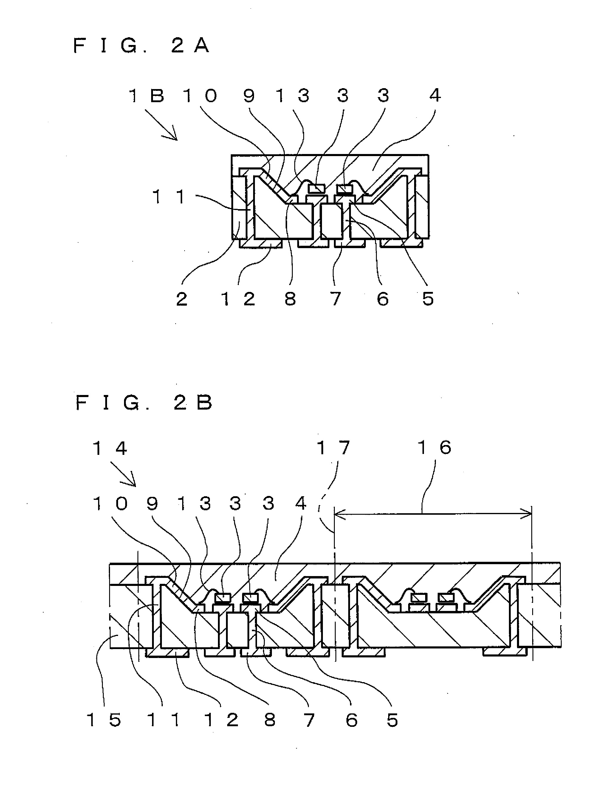
[0057]With reference to FIGS. 2A and 2B, a second embodiment regarding the resin-sealed light emitting device in the present invention will be described. FIGS. 2A and 2B are front vertical sectional views showing a resin-sealed light emitting device according to this embodiment and a sealed body as an intermediate body in a production process of the resin-sealed light emitting device shown in FIG. 2A, respectively.

[0058]According to this embodiment, as shown in FIG. 2A, plurality of LED chips 3 are mounted in a recessed part (having no reference numeral) provided in one surface (an upper surface in the drawing) of substrate 2. More specifically, one LED chip 3 is mounted on each of three setting patterns 5 provided in the recessed part. Therefore, three LED chips 3 are mounted on the recessed part (only two of them are shown in the drawing). Thus, three LED chips 3 emit R, G and B lights, respectively. Thus, the light emitted from an LED package 1B is substantially white light as an...

third embodiment

[0062]With reference to FIG. 3, a third embodiment regarding the resin-sealed light emitting device according to the present invention will be described. FIG. 3 is a front vertical sectional view showing a resin-sealed light emitting device according to this embodiment.

[0063]As shown in FIG. 3, according to this embodiment, a slanted surface provided on a side surface of a recessed part is a curved surface 18. Thus, wiring pattern 10 serving also as the light reflection part is formed on this curved surface. Thus, light emitted from LED chip 3 can be efficiently reflected upward by the light reflection part when a curvature of curved surface 18 is appropriately set. Therefore, according to this embodiment, in addition to the same characteristics in the first embodiment, LED package 1A has superior luminance efficiency.

[0064]Here, a method for forming curved surface 18 provided on the side surface of the recessed part will be described. When the silicon substrate is used, curved surf...


PUM

PropertyMeasurementUnit
diameteraaaaaaaaaa
diameteraaaaaaaaaa
conductiveaaaaaaaaaa

Abstract

An LED package is formed by separating a sealed body containing a substrate having a plurality of regions into individual bodies. The LED package includes an LED chip mounted on a recessed part in an upper surface of a substrate, a sealing resin to cover an entire surface of the region, a setting pattern provided on a bottom surface of the recessed part to set the LED chip, a wiring pad provided on the bottom surface of the recessed part, a wiring pattern provided on a slanted surface of the recessed part and serving as a light reflection part also, a wire to connect an electrode of the LED chip to the wiring pad, an external terminal provided on a lower surface of the substrate, a connection part to connect the wiring pattern connected to the wiring pad to the external terminal, and a heat radiating pattern provided on a lower surface to radiate a heat generated in the LED chip outside the LED package. The setting pattern is connected to the heat radiating pattern through the connection part.

Description

[0001]This nonprovisional application is based on Japanese Patent Application No. 2007-287546 filed on Nov. 5, 2007 with the Japan Patent Office, the entire contents of which are hereby incorporated by reference.BACKGROUND OF THE INVENTION[0002]1. Field of the Invention[0003]The present invention relates to a resin-sealed light emitting device having excellent heat radiation characteristics and luminance efficiency, and its manufacturing method.[0004]2. Description of the Background Art[0005]A conventional method for producing a resin-sealed light emitting device (referred to as the “LED package” occasionally hereinafter) by sealing an LED chip with a translucent resin will be described.[0006]As a method for sealing the LED chip with a resin, a method for mounting an LED chip in each of a plurality of regions provided in a circuit substrate (referred to as the “substrate” occasionally hereinafter) and sealing the LED chips in a lump with a resin has been proposed (refer to Japanese ...

Claims


Application Information

Patent Timeline
Patent Type & Authority Applications(United States)
IPC IPC(8): H01L33/00H01L21/00H01L33/64H01L33/50H01L33/54H01L33/56H01L33/62
CPCB29C43/18B29C70/70H01L2924/10253H01L2224/45144H01L2924/01079B29L2011/0016H01L33/486H01L33/52H01L33/62H01L33/642H01L2224/32225H01L2224/48227H01L2924/00
Inventor KAWAKUBO, KAZUKI
Owner TOWA
Why Eureka
Try Eureka