High tin solder etching solution

a technology of high tin solder and etching solution, which is applied in the direction of electrical equipment, metal-working equipment, solid-state devices, etc., can solve the problems of non-uniformity of etching rate across the entire surface, severe limitations in the bath life of concentrated hcl solution, and industry problems

Inactive Publication Date: 2009-05-14
GLOBALFOUNDRIES INC
View PDF7 Cites 12 Cited by
  • Summary
  • Abstract
  • Description
  • Claims
  • Application Information

AI Technical Summary

Benefits of technology

[0023]contacting the substrate with an aqueous composition comprising cupric ions, preferably cupric chloride or copp

Problems solved by technology

This has presented a problem to the industry.
A further limitation of these solutions is that H2 gas is evolved during the tin etch process and in addition to safety precautions required in a high volume production operation, bubble formation on the tin surface being etched leads to non-uniformity in the etching rate across the entire surface if these bubbles are not freely liberated.
The bath life

Method used


Image

  • High tin solder etching solution
  • High tin solder etching solution
  • High tin solder etching solution

Examples


Embodiment Construction

)

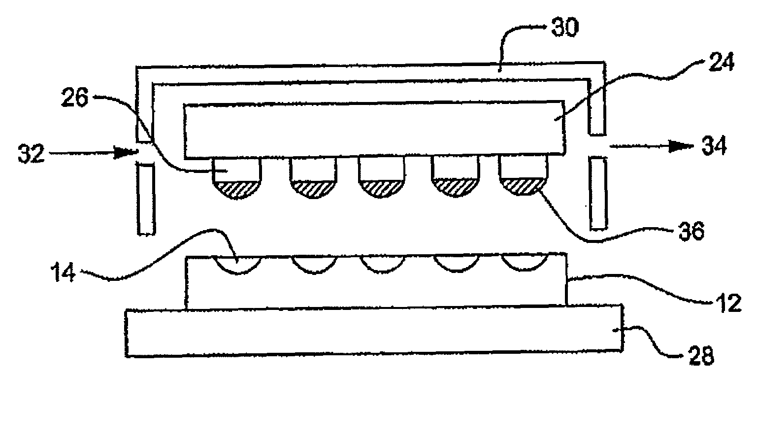
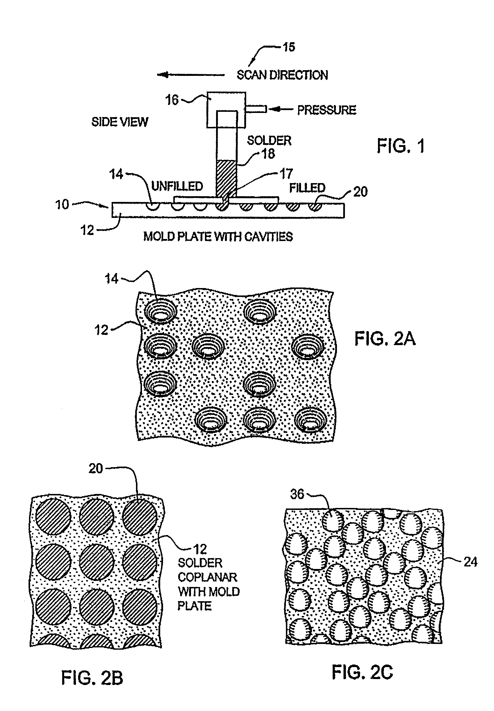
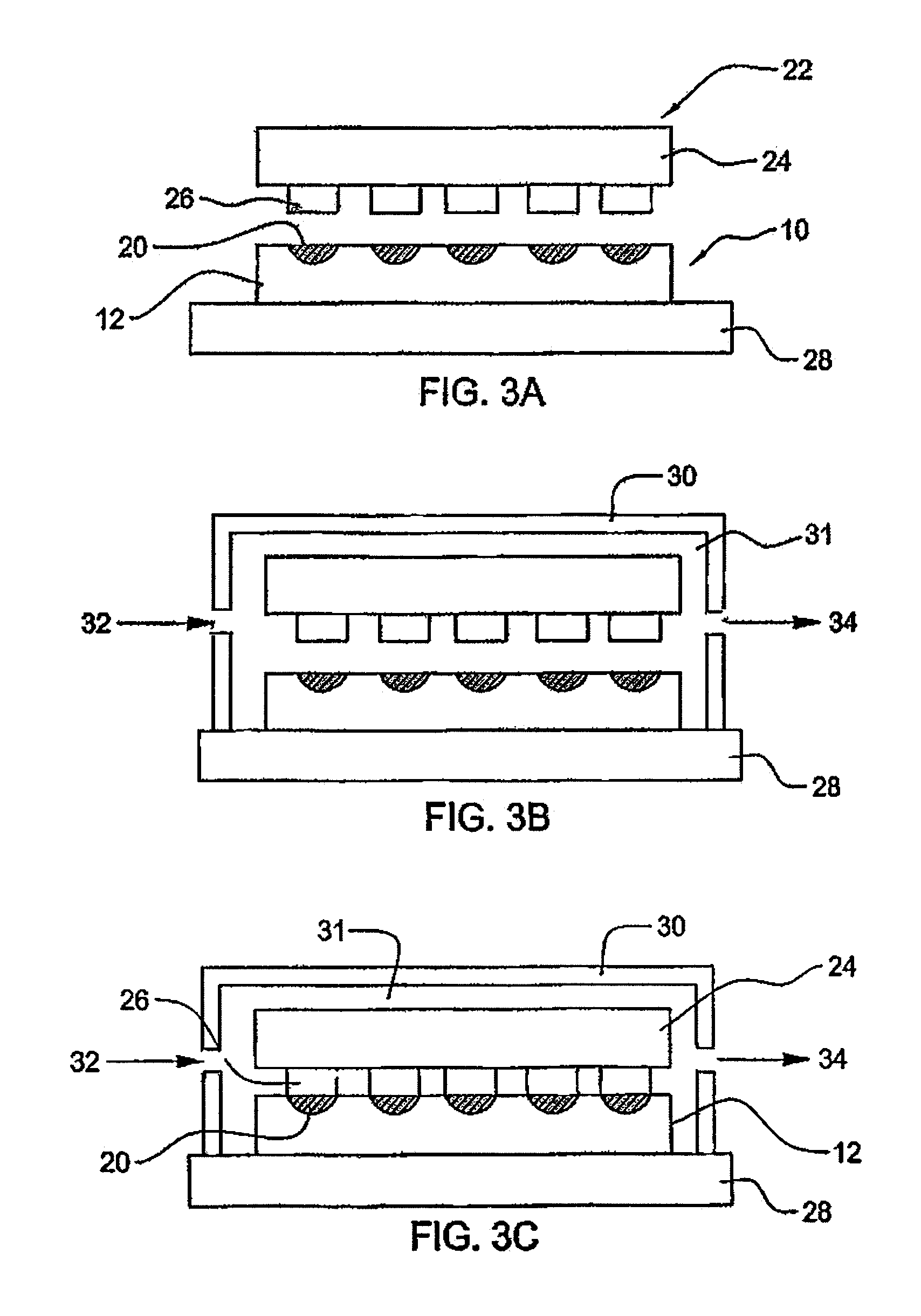
[0038]In describing the preferred embodiment of the present invention, reference will be made herein to FIGS. 1-3D of the drawings in which like numerals refer to like features of the invention.

[0039]Solder transfer molds using various solders containing tin may be readily processed using the method of the invention and the solders include lead-free binary, ternary and quaternary alloys. Lead-free alloys are of particular commercial significance and for convenience, the following description will be directed to such lead-free alloys, although it will be appreciated by those skilled in the art that any suitable solder may be readily processed using the method of the invention. Exemplary lead-free alloys include Sn-3.8% Ag-0.7% Cu, Sn-1.8% Ag, Sn-0.5% Ag and Sn-0.7% Cu. Also, in particular, the following description will be directed to tin containing lead-free alloys since these are likewise of significant commercial interest and an efficient method of providing solder interconnects ...


PUM

PropertyMeasurementUnit
Molar densityaaaaaaaaaa

Abstract

A method is provided for the removal of tin or tin alloys from substrates such as the removal of residual tin solder from the molds used in the making of interconnect solder bumps on a wafer or other electronic device. The method is particularly useful for the well-known C4NP interconnect technology and uses an etchant composition comprising cupric ions and HCl. Cupric chloride and cupric sulfate are preferred. A preferred method regenerates cupric ions by bubbling air or oxygen through the etchant solution during the cleaning process.

Description

BACKGROUND OF THE INVENTION[0001]1. Field of the Invention[0002]The present invention relates to the removal of tin or tin alloys from substrates and, in particular, to the making of interconnect solder bumps on a wafer or other electronic device using methods such as the well-known C4NP interconnect technology in which residual tin or tin alloy is removed from the transfer molds used in the C4NP method.[0003]2. Description of Related Art[0004]While the method of the invention is applicable to the removal of tin or tin alloy from any substrate the invention will be described for convenience to the removal of high tin composition solder from electronic substrates and in particular from the transfer molds used in the C4NP interconnect technology method.[0005]Forming an electronic package assembly whereby an electrical component such as an integrated circuit chip is electrically and mechanically connected to a substrate, a card, or board, another chip or another electronic part is well...

Claims


Application Information

Patent Timeline
IPC IPC(8): B23K31/02B08B3/04C09K13/04
CPCB23K1/0016B23K3/0623B23K35/262B23K35/3601B23K2203/08H05K2203/0338C23F1/44C23G1/10H05K3/26H05K3/3478H05K2203/0113C23F1/30B23K2103/08
Inventor INDYK, RICHARD F.SEMKOW, KRYSTYNA W.
Owner GLOBALFOUNDRIES INC
Why Eureka
Try Eureka