
Semiconductor device and method of fabricating the same

a semiconductor and semiconductor technology, applied in the field of semiconductor devices, can solve the problems of limited miniaturization limited high operating speed of a semiconductor product, and various limitations of typical wire bonding technology, and achieve the effect of reducing melting point and high oxidation resistan

Inactive Publication Date: 2009-05-14
SAMSUNG ELECTRONICS CO LTD
View PDF5 Cites 55 Cited by
  • Summary
  • Abstract
  • Description
  • Claims
  • Application Information

AI Technical Summary

Benefits of technology

[0029]In still other exemplary embodiments, the forming of the through electrode may include forming an external pattern in the first and second via holes and forming an internal pattern in a concave region surrounded by the external pattern, wherein the external pattern is formed of a conductive material having a higher oxidation resistance than that of the interna

Problems solved by technology

However, a typical wire bonding technology faces various limitations.
For example, since a certain amount of space is required for wire bonding, miniaturization of a semiconductor product is limited thereby.
Additionally, signal delay due to a wire length occurs such that a high operating speed of a semiconductor product is also limited.
As a result, manufacturing processes of a semiconductor product becomes complex and the miniaturization of the semiconductor product also becomes limited.
However, there exists various limitations in this case.
Accordingly, a reliability of the stacked semiconductor devices may be deteriorated.
Furthermore, a total thickness of the stacked semiconductor devices increases due to the bump.
Furthermore, terminals and / or bumps of a semiconductor device, made of copper or aluminum, oxidize easily.
As a result, because the additional processes for applying and removing the flux are necessary, a productivity of the semiconductor product is substantially reduced.
Additionally, the remaining flux may not be completely removed during the flux removal process.
For that reason, the reliability of a semiconductor product further deteriorates.

Method used


Image

  • Semiconductor device and method of fabricating the same
  • Semiconductor device and method of fabricating the same
  • Semiconductor device and method of fabricating the same

Examples


Embodiment Construction

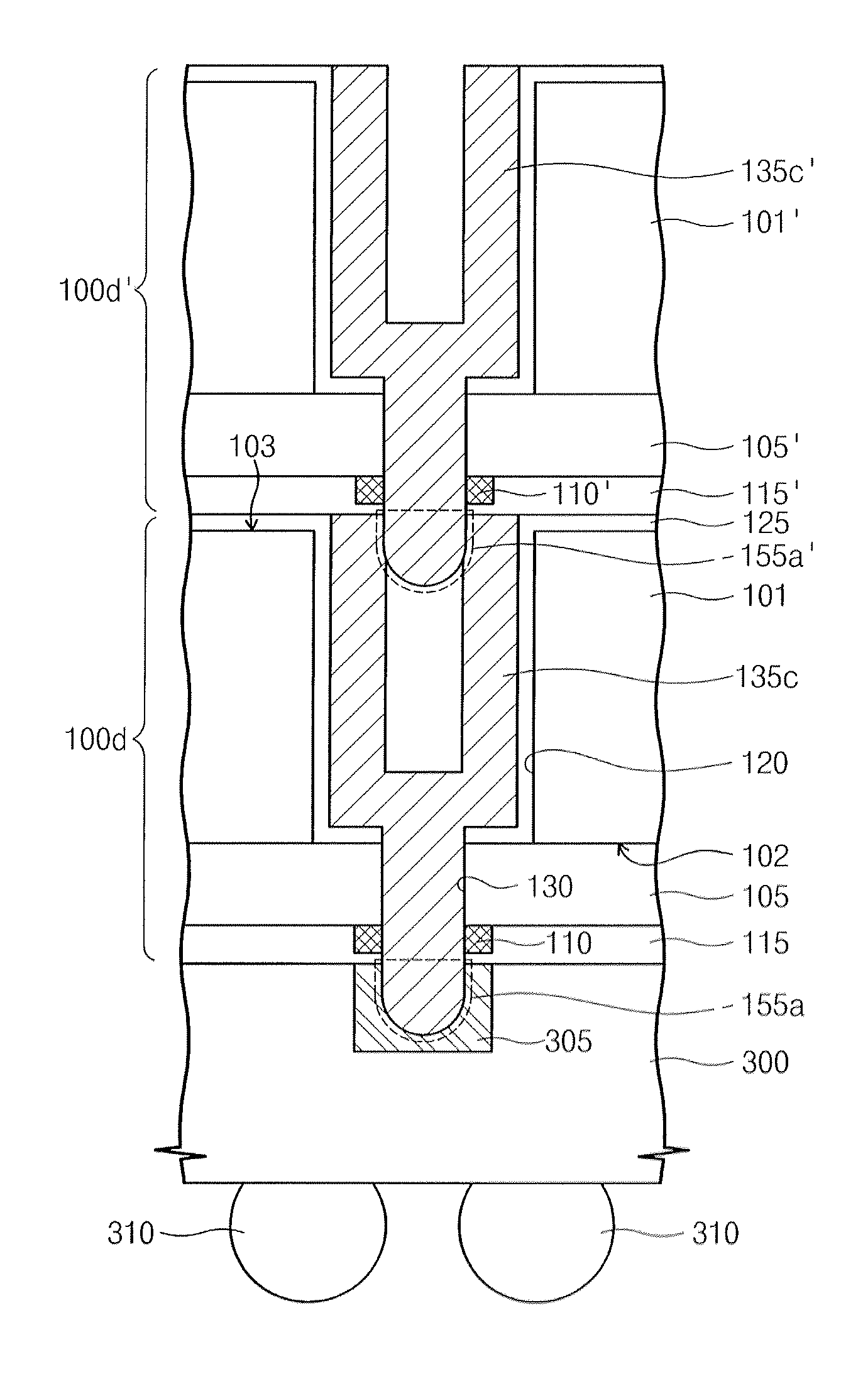
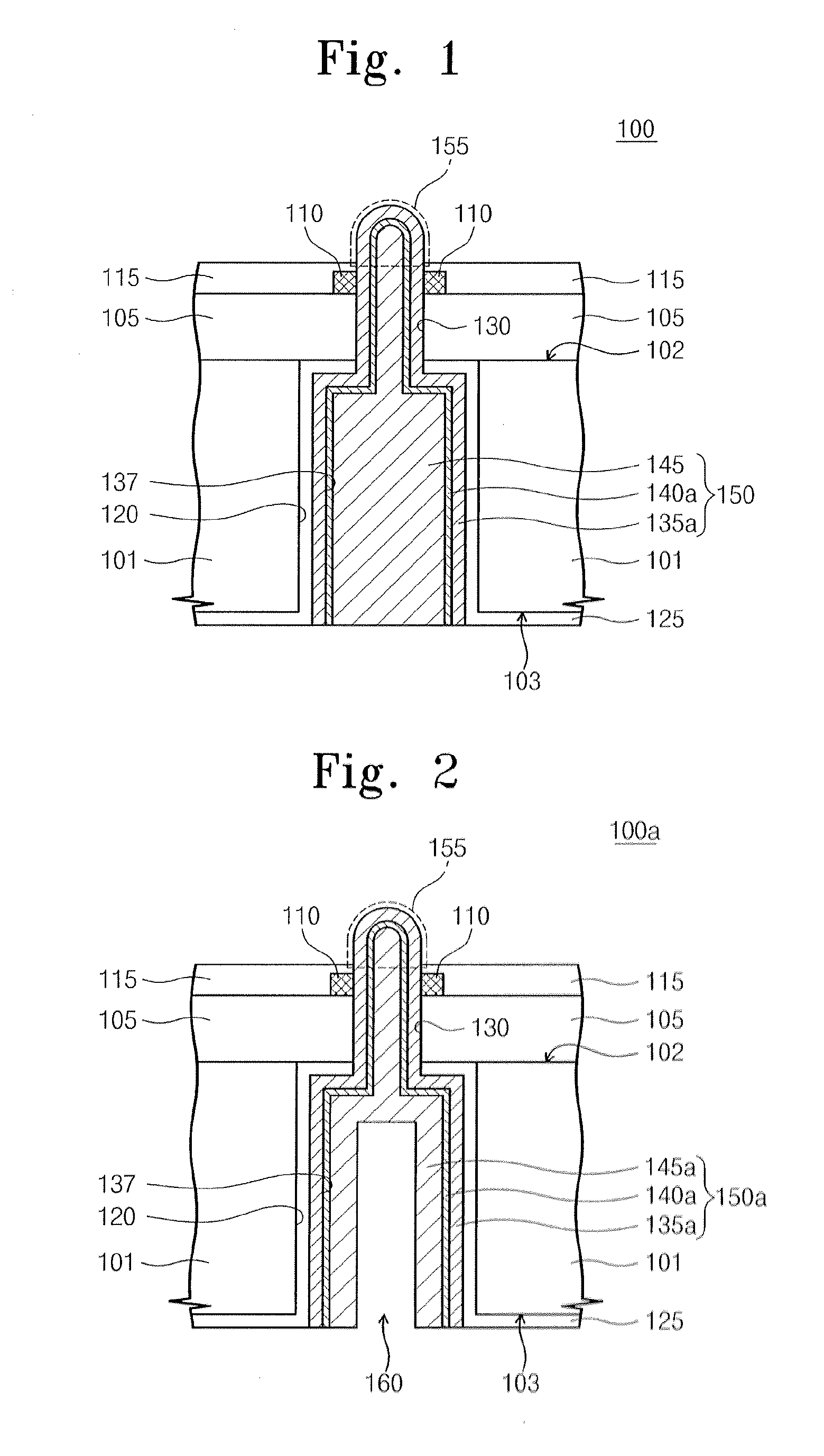
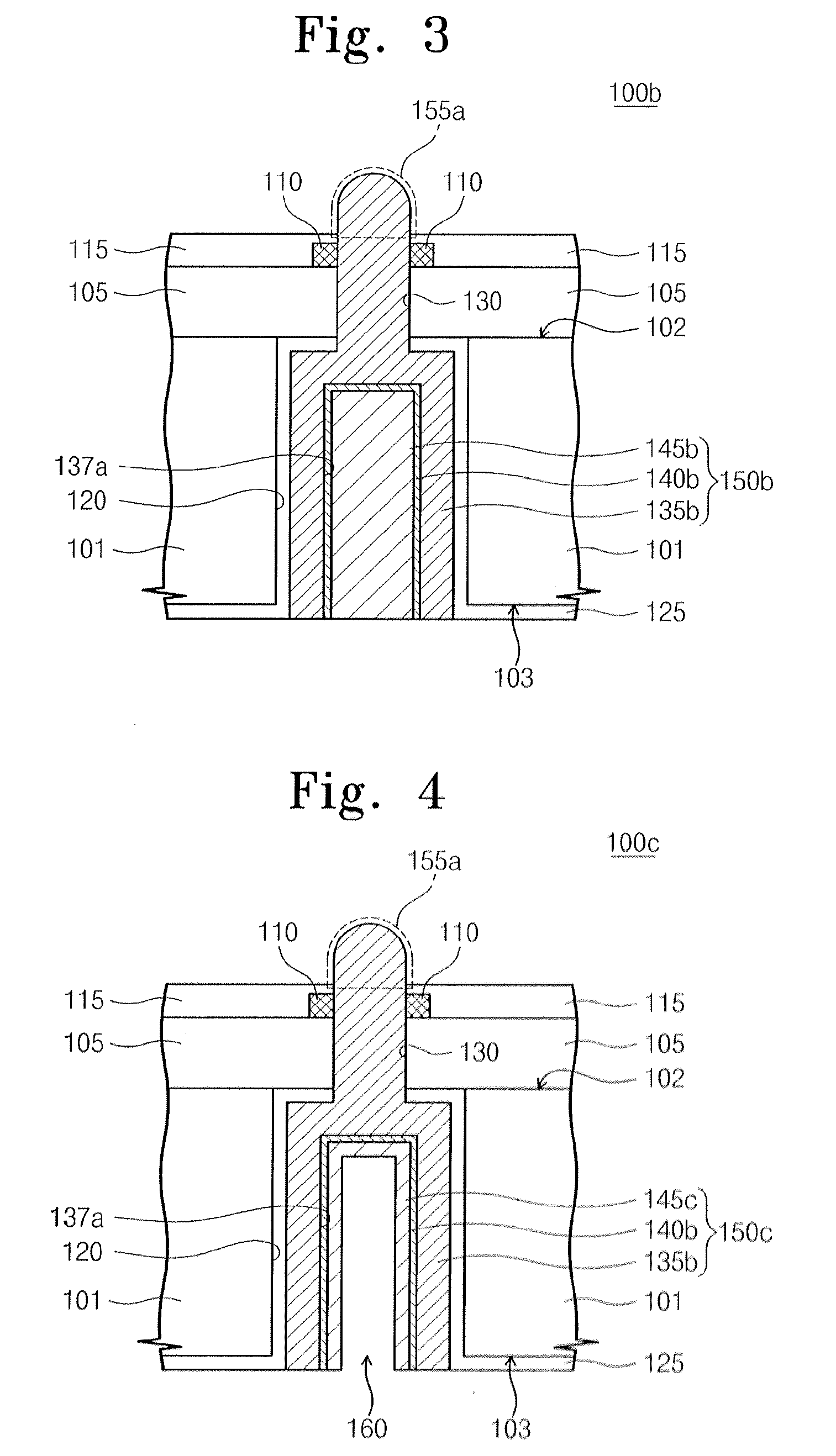
[0042]Preferred exemplary embodiments of the present general inventive concept will be described below in more detail with reference to the accompanying drawings. The present general inventive concept may, however, be embodied in different forms and should not be construed as limited to the exemplary embodiments set forth herein. Rather, these exemplary embodiments are provided so that this disclosure will be thorough and complete, and will fully convey the scope of the present general inventive concept to those skilled in the art. In the drawings, the thickness of a layer (or film) and regions are exaggerated for clarity. It will also be understood that when a layer (or film) is referred to as being ‘on’ another layer or substrate, it can be directly on the other layer or substrate, or intervening layers may also be present. Also, it will be understood that when a layer is referred to as being “formed on” another layer or substrate, it may also be “disposed on” the other layer or s...


PUM


Abstract

A semiconductor device and a method of fabricating the same. The semiconductor device includes a semiconductor substrate including an active surface and an inactive surface which faces the active surface, a device isolation layer and a pad stacked on the active surface; and a through electrode disposed in a first via hole and a second via hole and including a protruding part that protrudes from the pad, the first via hole penetrating the semiconductor substrate, the second via hole penetrating the device insulation layer and the pad continuously, wherein at least a surface of the protruding part of the through electrode is formed of an oxidation resistance-conductive material.

Description

CROSS-REFERENCE TO RELATED APPLICATIONS[0001]This U.S. non-provisional patent application claims priority under 35 U.S.C. § 119 from Korean Patent Application No. 10-2007-0113799, filed on Nov. 8, 2007, the disclosure of which is incorporated herein in its entirety by reference.BACKGROUND[0002]1. Field of the Invention[0003]The present general inventive concept relates to a semiconductor device and a method of fabricating the same, and more particularly, to a stackable semiconductor device, and a method of fabricating the same.[0004]2. Description of the Related Art[0005]Since a semiconductor industry has been highly developed, demands for low weight, miniaturized, and high speed semiconductor products have steadily increased. In addition to that, demands for multi-functional semiconductor products which are used for multiple functions have also gradually increased. In order to meet these demands, a method of further reducing a size, a minimum weight, a width of a semiconductor patt...

Claims


Application Information

Patent Timeline
IPC IPC(8): H01L23/48
CPCH01L21/76898H01L23/481H01L25/0657H01L25/50H01L2224/16H01L2225/06517H01L2225/06541H01L2924/15311H01L2225/06513H01L23/12H01L23/48
Inventor KWON, YONG-CHAIKIM, NAM-SEONG
Owner SAMSUNG ELECTRONICS CO LTD
Features
  • Generate Ideas
  • Intellectual Property
  • Life Sciences
  • Materials
  • Tech Scout
  • Unparalleled Data Quality
  • Higher Quality Content
  • 60% Fewer Hallucinations
Learn More