Board adapted to mount an electronic device, semiconductor module and manufacturing method therefore, and portable device
Active Publication Date: 2009-05-14
SANYO ELECTRIC CO LTD
2 Cites 6 Cited by
AI-Extracted Technical Summary
Problems solved by technology
With this flip-chip method, however, there are restrictive factors for the narrowing of the pitch of electrodes, such as the size of the solder bump itself and the bridge formation at soldering.
As a result, the stress may cause da...
View moreMethod used
[0065]The bump electrode 16 penetrates an insulating resin layer 70 and is electrically connected to an element electrode 52 provided in the semiconductor device 50. With the provision of the covering 18 on the bump electrode 16, the stress caused at the interface between the covering 18 and the element electrode 52 due to a change in temperature is dispersed under conditions where the semiconductor device 50 is mounted on the board 10. That is, the value of the maximum stress acting on the element electrode 52 can be reduced. As a result, the possibility of damaging the element electrode 52 is reduced and the connection reliability between the covering 18 and the element electrode 52 is improved.
[0072]Next, as illustrated in FIG. 2D, the covering 18 is formed on an exposed region of the bump electrode 16. The covering 18 is formed by electrolytic plating or electroless plating as a Au/Ni metal layer, using the resist 78 as a mask, for instance. As the covering 18 is formed by electrolytic plating or electroless plating as an Au/Ni metal layer, the direction of crystal grains of a metal that forms the covering 18 is aligned in a vertical direction to the contact surface of the element electrode 52. Accordingly, the pressure against the element electrode 52 at the time when the covering 18 is press-bonded to the element electrode 52 can be absorbed by the covering 18. As a result, the possibility of damaging the element electrodes 52 can be reduced. The covering 18 is formed by electrolytic plating or electroless plating. As a result, it can be formed at lower cost compared with a case where it is formed by a sputtering and the like. A metal layer that constitutes the covering 18 is formed so that a Ni layer lies on a side in contact with the bump electrode 16 and an Au layer lies on a side in contact with the element electrode 52. Note that the method for forming the covering 18 is not limited to the above-described one and, for example, it may be formed using conducive paste such as copper paste, silver paste and gold paste.
[0078]Next, as illustrated in FIG. 3C, resists 80 are selectively formed according to the patterns of wiring layer 14 by the lithography method. More specifically, a resist film of a predetermined thickness is affixed to the copper sheet 13 by a laminator unit, and it is then exposed using a photo mask having the patterns of wiring layer 14. After this, the resists in the unexposed areas are removed by a development using a Na2CO3 solution, which will selectively form the resists 80 on the copper sheet 13. To improve the adhesion of the resists 80 to the copper sheet 13, it is desirable that a pretreatment, such as grinding, cleaning and the like, be performed as appropriate on the surface of the copper sheet 13 before the lamination of the resist film thereon. Before the lamination of the resist film, the copper sheet 13 may be adjusted into the thickness of the wiring layer 14 by etching the whole of the opposite side of the copper sheet 13.
[0085]The top surface of the bump electrode 16 and the region, at a side surface thereof, continuous with the top surface thereof excluding a region in contact with the wiring layer 14 are covered or coated, so that the stress caused at the interface between the covering 18 and the element electrode 52 disperses. Thus, as shown in FIG. 5, it is evident that the value of the maximum stress occurring in the element electrode 52 can be reduced. If the yield stress of the covering 18 is greater than 40% and less than or equal to 100% of the yield stress of the bump electrode, there exists a local minimal value of the maximum stress. Thus, it is found that it is possible to effectively control the stress acting on the interface between the covering 18 and the bump electrode 16 if the yield stress is greater than 40% and less than or equal to 100%. If the height h of the covering is 0 μm or 40 μm which is the same as the height of the bump electrode 16, in theory this is the same situation as when no covering is provided. In the light of this, the values of the maximum yield stress for the covering 18 having different heights (greater than 0 μm and less than 40 μm) are compared against those for the covering 18 having 0 μm and 40 μm as their references. As a result, it is found that when the yield stress is greater than or equal to 50% and less than or equal to 75% and the height of the covering is less than or equal to ½ of the height of the bump electrode 16, the maximum stress occurring in the interface between the covering 18 and the bump electrode 16 can be made smaller.
[0088]As described above, by employing this first embodiment, the coverings 18 are provided on the bump electrodes 16, so that the position where the stress caused by the temperature change is concentrated can be moved from the interface between the covering 18 and the element electrode 52 to a bump electrode 16 side. As a result, the maximum stress occurring in the interface can be made smaller. Thus, when the semiconductor device 50 is mounted on the packaging board 10, the possibility of damaging the element electrodes 52 is reduced and the connection reliability between the bump electrode 16 and the element electrode 52 is improved. Furthermore, the connection reliability between the board 10 and the semiconductor device 50 is improved. Also, the provision of the coverings prevents the semiconductor device 50 from getting broken, so that the yield of the semiconductor modules 30 can be enhanced and the manufacturing cost of semiconductor modules 30 can be reduced.
[0095]According to the second embodiment, the following advantageous effects are achieved in addition to those of the first embodiment. That is, ...
View moreBenefits of technology
[0008]The present invention has been made in view of the foregoing circumstances, and a general purpose thereof is to provide a technology for reducing the possibility of damaging the electrodes of a semiconductor device and improving the connection reliability be...
View moreAbstract
A board adapted to mount an electronic device includes an insulating resin layer, a wiring layer of a predetermined pattern provided on one surface of the insulating resin layer, a bump electrode provided on an insulating-resin-layer-side surface of the wiring layer, and a covering, formed of a metal layer, which covers a top surface of the bump electrode and a region, at a side surface of the bump electrode, continuous with the top surface excluding a region in contact with the wiring layer.
Application Domain
Technology Topic
Image
Examples
- Experimental program(11)
Example
First Embodiment
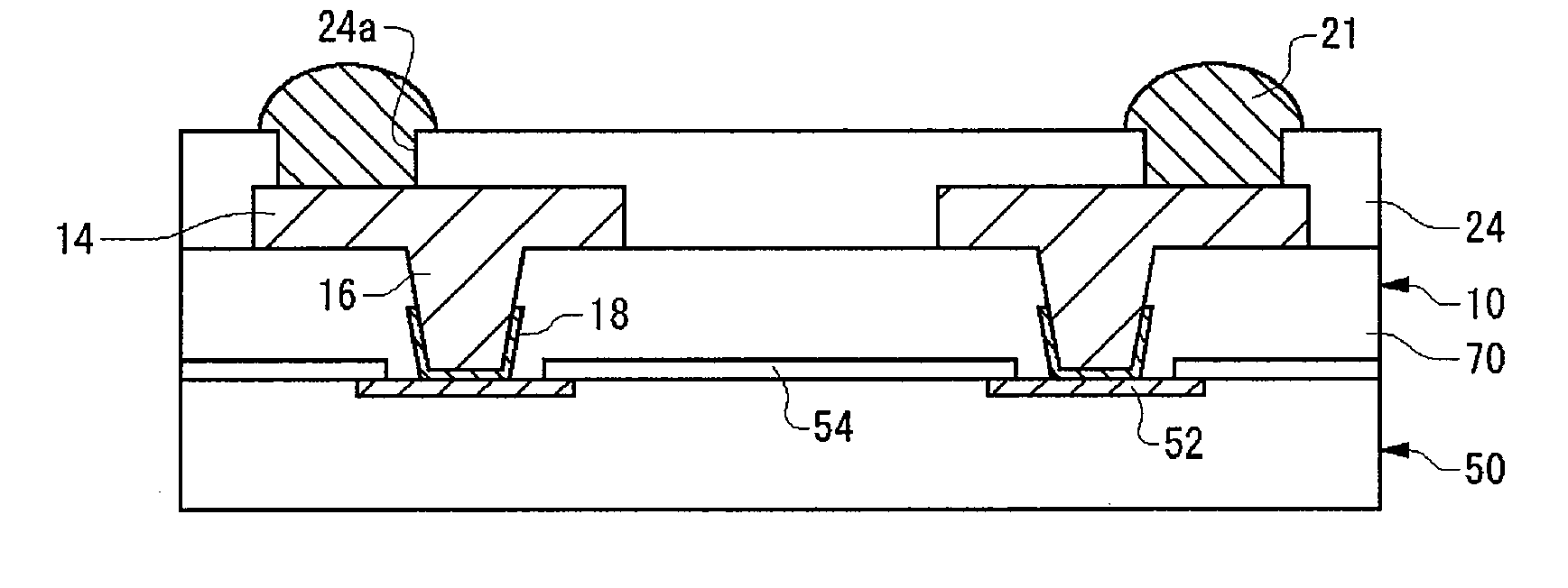
[0056]FIG. 1 is a schematic cross-sectional view illustrating a structure of a board adapted to mount an electronic device 10 according to first embodiment of the present invention and that of a semiconductor module 30 using said board 10. The semiconductor module 30 is comprised of a board adapted to mount an electronic device 10 and a semiconductor device 50 mounted on the board 10. It is to be noted that in the embodiments described hereinbelow, a “board adapted to mount an electronic device 10” is referred to as “packaging board 10” or simply as “board 10” also.
[0057]The board 10 includes an insulating resin layer 70, a wiring layer 14 provided on one face of the insulating resin layer 70, a bump electrode 16 provided on a surface of the wiring layer 14 on an insulating resin layer 70 side thereof, and a covering 18 which covers or coats a top surface of the bump electrode 16 and a region, at a side surface thereof, continuous with the top surface thereof excluding a region in contact with the wiring layer 14.
[0058]The insulating resin layer 70 is made of a material that develops plastic flow when pressurized. An example of the material that develops plastic flow when pressurized is epoxy thermosetting resin. The epoxy thermosetting resin to be used for the insulating resin layer 70 may be, for example, one having viscosity of 1 kPa·s under the conditions of a temperature of 160° C. and a pressure of 8 MPa. If a pressure of 5 to 15 MPa is applied to this epoxy thermosetting resin at a temperature of 160° C., then the viscosity of the resin will drop to about ⅛ of the viscosity thereof with no pressurization. In contrast to this, an epoxy resin in B stage before thermosetting has no viscosity, similarly to a case when the resin is not pressurized, under a condition that the temperature is less than or equal to a glass transition temperature Tg. And the epoxy resin develops no viscosity even when pressurized under a condition that the temperature is less than or equal to a glass transition temperature Tg.
[0059]In the semiconductor module 30 according to the first embodiment, the insulating resin layer 70 is provided between the wiring layer 14 and the semiconductor device 50. One face of the insulating resin layer 70 is press-bonded to the wiring layer 14 whereas the other face thereof is press-bonded to the semiconductor device 50. A material that develops plastic flow when pressured is used for the insulating resin layer 70 in the present embodiment. As a result, when the packaging board 10, the insulating resin layer 70, and the semiconductor device 50 are press-bonded in this order and united into one body, the probability that a residual film of insulating resin layer 70 will stay on at an interface between a covering 18 and an element electrode 52 is suppressed. Hence, the connection reliability is improved.
[0060]The wiring layer 14 is formed by a conductive material, preferably a rolled metal or more preferably by a rolled copper. A wiring protective layer 24 is provided on a surface of the insulating resin layer 70 opposite to the wiring layer 14. This wiring protective layer 24 protects the wiring layer 14 against oxidation or the like. The wiring protective layer 24 is formed of a photo solder resist, for instance. An opening 24a is formed in a predetermined position of the wiring protective layer 24 so that the wiring layer 14 is exposed. And a solder bump 21 is formed on the wiring layer 14 thus exposed in the opening 24a. The position of the opening 24a, namely, the position in which the solder bump 21 is formed is, for instance, a targeted position where circuit wiring is extended through a rewiring.
[0061]In the wiring layer 14, the bump electrodes 16 are provided in positions corresponding respectively to the element electrodes 52 of the semiconductor device 50. In the first embodiment, the wiring layer 14 and the bump electrode 16 are formed integrally with each other. The planar view of the bump electrode 16 is a round shape, and the bump electrode has a side surface which is shaped with a diameter smaller toward a head portion. However, the shape of the bump electrode 16 is not limited to any particular shape and may be, for instance, in the shape of a cylinder with a predetermined diameter. Also, the bump electrode 16 may be polygonal, such as quadrangular, when viewed planarly.
[0062]The covering 18 is provided on the top surface of the bump electrode 16 and on a region, at a side surface thereof, continuous with the top surface thereof excluding a region in contact with the wiring layer 14. More specifically, the covering 18 is a metal plating layer which is formed, by electrolytic plating or electroless plating, using a metal material having a yield stress which is, for example, greater than 40% of the yield stress of the bump electrode 16 and less than or equal to 100% of that of the bump electrode. Or the covering 18 may be a conductive paste layer formed using a conductive paste. The metal layer may be multilayered and may be stacked with a Ni plating layer and an Au plating layer, for example. In the first embodiment, such layers are a Ni/Au plating layer formed of gold (Au) and nickel (Ni) having 60% of the yield stress relative to the yield stress of the bump electrode 16 formed of copper.
[0063]If the bump electrode 16 and the covering 18 are formed of the same material, the bump electrode 16 and the covering 18 may be formed integrally with each other. In such a case, the bump electrode 16 is of a shape having a stepped portion on the side surface thereof such that the stepped portion on a wiring layer 14 side is thinner.
[0064]In the first embodiment, the covering 18 covers or coats the top surface of the bump electrode 16 and a top-surface-side region of each side surface which is less than or equal to one half of the height of the bump electrode 16 measured from the top surface thereof to a surface of the wiring layer 14 where the bump electrode 16 is provided. Here, if one surface of the wiring layer 14 where the bump electrode is provided, namely the surface thereof which serves as one of reference surfaces for the height of the bump electrode 16, has fine roughness or fine asperities on the wiring layer 14, the surface thereof will be defined to be a surface that passes through the average height of these fine asperities, for instance. Similarly, if the top surface of the bump electrode 16, which serves as the other reference surface for the height of the bump electrode 16, has fine asperities thereon, the top surface thereof will be defined to be a surface that passes through the average height of these fine asperities.
[0065]The bump electrode 16 penetrates an insulating resin layer 70 and is electrically connected to an element electrode 52 provided in the semiconductor device 50. With the provision of the covering 18 on the bump electrode 16, the stress caused at the interface between the covering 18 and the element electrode 52 due to a change in temperature is dispersed under conditions where the semiconductor device 50 is mounted on the board 10. That is, the value of the maximum stress acting on the element electrode 52 can be reduced. As a result, the possibility of damaging the element electrode 52 is reduced and the connection reliability between the covering 18 and the element electrode 52 is improved.
[0066]The semiconductor device 50 is press-bonded to the insulating resin layer 70 in a manner such that an electrode surface of the semiconductor device 50 provided with the element electrodes 52 is disposed toward an insulating resin layer 70 side. A protective layer 54 of the semiconductor device 50 is stacked on the semiconductor device 50 wherein the protective layer 50 has openings for the element electrodes 52. A specific example of the semiconductor device 50 is a semiconductor chip such as an integrated circuit (IC) or a large-scale integrated circuit (LSI). A specific example of the protective layer 54 is a polyimide layer. For example, aluminum is used as the element electrode 52.
[0067](Manufacturing Method of Semiconductor Module)
[0068]FIGS. 2A to 2E are cross-sectional views showing a process in a method for forming the bump electrodes 16 and the coverings 18.
[0069]As shown in FIG. 2A, a copper sheet 13 having the thickness at least larger than the sum of the height of the bump electrode 16 and the thickness of the wiring layer 14 is prepared as a metal sheet.
[0070]Then, as shown in FIG. 2B, a resist (not shown) is selectively formed on an electrode forming area by a lithography method, and bump electrodes 16 of a predetermined pattern is formed on the copper sheet 13 using the resist as a mask. The bump electrodes 16 are provided in positions corresponding respectively to the positions of element electrodes 52 formed on the semiconductor device 50 (See FIG. 3A).
[0071]Next, as shown in FIG. 2C, a resist 78 is stacked on a main surface S1 side of the copper sheet 13 up to a predetermined height. The height of the stacked resist 78 corresponds to the height of a region coated with the covering 18 discussed later. More specifically, the height of the resist 78 corresponds to the height of an exposed region. Here, this exposed region is a region where the top surface of the bump electrode 16 and a top-surface-side region of the side surface thereof which is less than or equal to one half of the height of the bump electrode 16 measured from the top surface thereof to a surface of the copper sheet 13, where the bump electrode 16 is provided, are exposed.
[0072]Next, as illustrated in FIG. 2D, the covering 18 is formed on an exposed region of the bump electrode 16. The covering 18 is formed by electrolytic plating or electroless plating as a Au/Ni metal layer, using the resist 78 as a mask, for instance. As the covering 18 is formed by electrolytic plating or electroless plating as an Au/Ni metal layer, the direction of crystal grains of a metal that forms the covering 18 is aligned in a vertical direction to the contact surface of the element electrode 52. Accordingly, the pressure against the element electrode 52 at the time when the covering 18 is press-bonded to the element electrode 52 can be absorbed by the covering 18. As a result, the possibility of damaging the element electrodes 52 can be reduced. The covering 18 is formed by electrolytic plating or electroless plating. As a result, it can be formed at lower cost compared with a case where it is formed by a sputtering and the like. A metal layer that constitutes the covering 18 is formed so that a Ni layer lies on a side in contact with the bump electrode 16 and an Au layer lies on a side in contact with the element electrode 52. Note that the method for forming the covering 18 is not limited to the above-described one and, for example, it may be formed using conducive paste such as copper paste, silver paste and gold paste.
[0073]Then, as shown in FIG. 2E, the resist 78 is removed. The bump electrodes 16 and the coverings 18 are formed through the above-described processes.
[0074]In the first embodiment, the diameter of the bump electrode 16 at the bottom face of a wiring layer 14 side, and the diameter of the bump electrode 16 at the top surface and the height of the bump electrode 16 are 40 nmφ, 30 μmφ and 40 μmφ, respectively. The thickness of the covering 18 is 5 μm; and of 5 μm, 1 μm is the thickness of the Au layer and 4 μm is the thickness of the Ni layer. The range of the covering 18 that covers a side surface of the bump electrode 16 is indicated by a region whose height measured from the top surface of the bump electrode 16 is less than or equal to 20 μm.
[0075]FIGS. 3A to 3D and FIGS. 4A and 4B are cross-sectional views showing a process in a method for connecting the bump electrodes 16 and the element electrodes 52.
[0076]As shown in FIG. 3A, an insulating resin layer 70 is held between a semiconductor device 50 where element electrodes 52 having predetermined patterns are formed and a copper sheet 13 formed using the above-described method. The film thickness of the insulating resin layer 70 is approximately equal to the height of the bump electrode 16 and is about 40 μm.
[0077]As shown in FIG. 3B, the semiconductor device 50, the insulating resin layer 70 and the copper sheet 13 are press-formed by a press machine into a single block. The pressure and the temperature for the press-forming are about 5 MPa and 180° C., respectively. The press-forming causes the bump electrodes 16 and the coverings 18 to penetrate the insulating resin layer 70. As a result, the coverings 18 are press-bonded to the element electrodes 52 and thus the bump electrodes 16 are electrically coupled with the element electrodes 52. The bump electrode 16 and the covering 18, whose overall shape is narrower toward the tip portion thereof, penetrates the insulating resin layer 70 smoothly.
[0078]Next, as illustrated in FIG. 3C, resists 80 are selectively formed according to the patterns of wiring layer 14 by the lithography method. More specifically, a resist film of a predetermined thickness is affixed to the copper sheet 13 by a laminator unit, and it is then exposed using a photo mask having the patterns of wiring layer 14. After this, the resists in the unexposed areas are removed by a development using a Na2CO3 solution, which will selectively form the resists 80 on the copper sheet 13. To improve the adhesion of the resists 80 to the copper sheet 13, it is desirable that a pretreatment, such as grinding, cleaning and the like, be performed as appropriate on the surface of the copper sheet 13 before the lamination of the resist film thereon. Before the lamination of the resist film, the copper sheet 13 may be adjusted into the thickness of the wiring layer 14 by etching the whole of the opposite side of the copper sheet 13.
[0079]As shown in FIG. 3D, etching is done to an exposed part of the copper sheet 13, using a ferric chloride solution to form wiring layers 14 having predetermined wiring patterns. Then the resists 80 are removed using a stripping agent, such as an NaOH solution. In the first embodiment, the thickness of the wiring layer 14 is 15 μm.
[0080]Then, as shown in FIG. 4A, a wiring protective layer 24 having an opening 24a is stacked on the wiring layer 14 at the side opposite to the insulating resin layer 70.
[0081]Then, as shown in FIG. 4B, a solder bump 21 is formed on the wiring layer 14 which is exposed in the opening 24a. The position in which the solder bump 21 is to be formed may be a targeted position where circuit wiring is extended through a rewiring.
[0082]By employing the above-described manufacturing process, a semiconductor module 30 is obtained. If the semiconductor device 50 is not stacked, the board 10 will be obtained.
[0083]A description is given hereunder of advantageous effects of the present embodiment obtained by providing the covering 18 on the bump electrode 16.
[0084]FIG. 5 is a graph showing a calculated relation (by Finite Element Method) between a region of formation of the covering 18 (the height of the covering) and the maximum stress caused at the interface between the covering 18 and the element electrode 52, for each covering 18 formed of a metal material of different yield stress in an atmosphere where the temperature varies from 25° C. to 125° C. The copper is used as a material that forms the bump electrode 16, and the relation is investigated when the yield stress of the metal material that forms the covering 18 varies from 25% to 150% of the yield stress of the bump electrode 16.
[0085]The top surface of the bump electrode 16 and the region, at a side surface thereof, continuous with the top surface thereof excluding a region in contact with the wiring layer 14 are covered or coated, so that the stress caused at the interface between the covering 18 and the element electrode 52 disperses. Thus, as shown in FIG. 5, it is evident that the value of the maximum stress occurring in the element electrode 52 can be reduced. If the yield stress of the covering 18 is greater than 40% and less than or equal to 100% of the yield stress of the bump electrode, there exists a local minimal value of the maximum stress. Thus, it is found that it is possible to effectively control the stress acting on the interface between the covering 18 and the bump electrode 16 if the yield stress is greater than 40% and less than or equal to 100%. If the height h of the covering is 0 μm or 40 μm which is the same as the height of the bump electrode 16, in theory this is the same situation as when no covering is provided. In the light of this, the values of the maximum yield stress for the covering 18 having different heights (greater than 0 μm and less than 40 μm) are compared against those for the covering 18 having 0 μm and 40 μm as their references. As a result, it is found that when the yield stress is greater than or equal to 50% and less than or equal to 75% and the height of the covering is less than or equal to ½ of the height of the bump electrode 16, the maximum stress occurring in the interface between the covering 18 and the bump electrode 16 can be made smaller.
[0086]FIGS. 6A and 6B are schematic diagrams showing calculated distributions (by Finite Element Method) of the stress caused in an atmosphere where the temperature varies from 25° C. to 125° C., in the bump electrodes 16 where the covering 18 having the yield stress of 50% and the covering height h of 10 μm (which is ¼ of the height of the bump electrode 16) and the covering having the yield stress of 50% and the covering height h of 40 μm (which is the same height as that of the bump electrode 16), respectively.
[0087]As shown in FIG. 6B, when the covering height h is the same as the height of the bump electrode 16, the stress is concentrated at the interface between the covering 18 and the element electrode 52. As shown in FIG. 6A, on the other hand, when the covering height h of the covering 18 is ¼ of the height of the bump electrode 16, the stress is concentrated on the interior of the bump electrode 16. In other words, the provision of the covering 18 enables the area, where the stress caused by the temperature change is concentrated, to migrate from the interface between the covering 18 and the element electrode 52 to the interior of the bump electrode 16. This can disperse the stress acting on the interface between the covering 18 and the element electrode 52, so that the maximum stress occurring in the interface thereof can be reduced.
[0088]As described above, by employing this first embodiment, the coverings 18 are provided on the bump electrodes 16, so that the position where the stress caused by the temperature change is concentrated can be moved from the interface between the covering 18 and the element electrode 52 to a bump electrode 16 side. As a result, the maximum stress occurring in the interface can be made smaller. Thus, when the semiconductor device 50 is mounted on the packaging board 10, the possibility of damaging the element electrodes 52 is reduced and the connection reliability between the bump electrode 16 and the element electrode 52 is improved. Furthermore, the connection reliability between the board 10 and the semiconductor device 50 is improved. Also, the provision of the coverings prevents the semiconductor device 50 from getting broken, so that the yield of the semiconductor modules 30 can be enhanced and the manufacturing cost of semiconductor modules 30 can be reduced.
Example
Second Embodiment
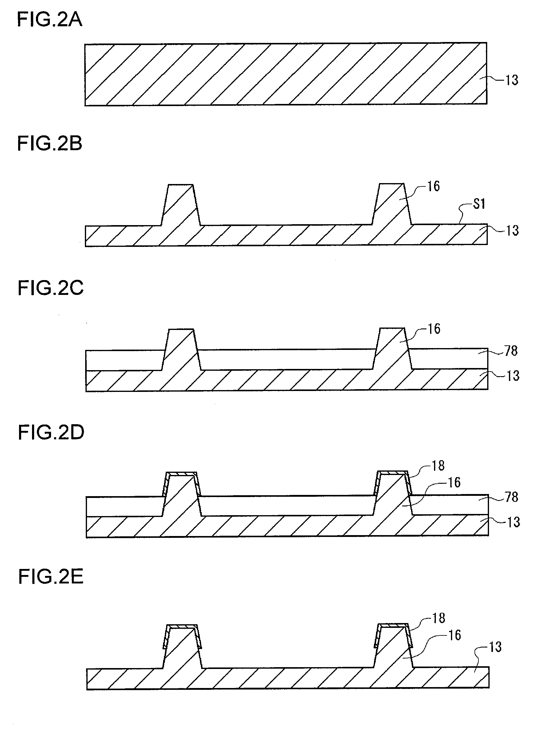
[0089]In the above-described first embodiment, the insulating resin layer 70 is held and press-formed between the copper sheet 13 and the semiconductor device 50 and thereby the semiconductor device 50, the insulating resin layer 70 and the copper sheet 13 are united into one body so as to form the semiconductor module 30. The semiconductor module 30 may also be formed as follows. Note that the other components in the semiconductor module 30, the method for manufacturing the bump electrodes 16 and the coverings 18, and the like are basically the same as those in the first embodiment and therefore the description thereof is omitted as appropriate.
[0090]FIGS. 7A to 7D are cross-sectional views showing a process in a method for manufacturing the semiconductor module 30 according to the second embodiment.
[0091]As shown in FIG. 7A, the above-described epoxy thermosetting resin 71 is stacked on the main surface S1 of one face of the copper sheet 13.
[0092]Then, as shown in FIG. 7B, a covering 18 is exposed by etching the epoxy thermosetting resin 71 so as to form an insulating resin layer 70. Then the copper sheet 13, on which the insulating resin layer 70 has been formed, and the semiconductor device 50 are press-formed so as to unite the semiconductor device 50, the insulating resin layer 70 and the copper sheet 13 into a single block as shown in FIG. 7C.
[0093]Then, as shown in FIG. 7D, by following the similar procedure as in the first embodiment, a wiring layer 14 is formed by etching the copper sheet 13; a wiring protective layer 24 having an opening 24a is laminated on a surface of the wiring layer 14 opposite to the insulating resin layer 70. Then, a solder bump 21 is formed on the wiring layer 14 which is exposed in the opening 24a.
[0094]By employing the above-described manufacturing process, a semiconductor module 30 is obtained. If the semiconductor device 50 is not stacked, the board 10 will be obtained.
[0095]According to the second embodiment, the following advantageous effects are achieved in addition to those of the first embodiment. That is, in the second embodiment the covering 18 is exposed from the insulating resin layer 70, so that the board 10 and the semiconductor device 50 can be accurately positioned when they are to be press-formed. At the same time, the connection reliability between the covering 18 and the element electrode 52 is improved. As a result, the connection reliability between the packaging board 10 and the semiconductor device 50 is further enhanced.
Example
Third Embodiment
[0096]Though the semiconductor module 30 is formed using a so-called pasting process in the above-described first embodiment, the semiconductor module 30 may be formed using a so-called buildup process as will be shown in the following third embodiment. Note that description of the other components similar to those of the first embodiment is omitted as appropriate.
[0097]FIGS. 8A to 8F and FIGS. 9A to 9C are cross-sectional views showing a process in a method for manufacturing a semiconductor module 30 according to the third embodiment.
[0098]As shown in FIG. 8A, a semiconductor device 50 in which an element electrode 52 of a predetermined pattern is formed is prepared.
[0099]Then, as shown in FIG. 8B, a resin layer 72 is stacked on a protective layer 54 of a semiconductor device 50. The resin layer 72 may be formed as follows. That is, the above-described epoxy thermosetting resin is laminated on the entire surface of the element electrode 52 side of the semiconductor device 50; the resin on the upper region of the element electrode 52 is etched; and thereby an opening 72a is provided. In this manner, the resin layer 72 is formed. The thickness (height) of the resin layer 72 corresponds to the height of a region coated with the covering 18. Then, a metallic coated film 18a is formed on the side of the semiconductor device 50, where the resin layer 72 has been stacked, by the sputtering or the like.
[0100]Then, as shown in FIG. 8C, a region of the coated film excluding the inner surface of the opening 72a is removed from the coated film 18a. As a result, the covering 18 is formed.
[0101]Then, as shown in FIG. 8D, the resin layer 73 made of the above-described epoxy thermosetting resin is stacked on the resin layer 72. In the resin layer 73, an opening 73a is provided above the opening 72a. The insulating resin layer 70 is formed as one block by the resin layer 72 and the resin layer 73. The resin layer 73 can be provided as follows, for instance. That is, a mask is provided in the opening 72a; the resin layer 73 is stacked; and then the mask is removed. Alternatively, the resin layer 73 may be provided as follows. That is, the epoxy thermosetting resin is laminated on the whole surface of one side of the semiconductor device 50 where the resin layer 72 has been stacked; a region excluding a part thereof in which the opening 72a is provided (an upper area of the element electrode 52) may be masked; and the openings 72a and 73a are formed.
[0102]Then, as shown in FIG. 8E, a bump electrode 16 is formed within the openings 72a and 73a. The bump electrode 16 can be formed by electrolytic plating or electroless plating, for instance. Or the bump electrode 16 can be formed using the copper paste.
[0103]Then, as shown in FIG. 8F, the copper sheet 22 is laminated on the whole surface of a resin layer 73 side of the semiconductor device 50.
[0104]Then, as shown in FIG. 9A, a resist (not shown) is selectively formed on a wiring layer forming area of the copper sheet 22 by the lithography method, and a wiring layer 14 of a predetermined pattern is formed using the resist as a mask.
[0105]Then, as shown in FIG. 9B, the wiring protective layer 24 having the opening 24a is laminated on the surface of the wiring layer 14 opposite to the insulating resin layer 70.
[0106]Then, as shown in FIG. 9C, the solder bump 21 is formed on the wiring layer 14 which is exposed in the opening 24a.
[0107]By employing the above-described manufacturing process, a semiconductor device 30 is obtained. If the semiconductor device 50 is not used, the board 10 will be obtained.
[0108]According to the third embodiment, the following advantageous effects are achieved in addition to those of the first embodiment. That is, when the semiconductor module 30 is to be formed using a buildup process as in the third embodiment, the board 10 and the semiconductor device 50 are not press-bonded together as in the pasting process. Hence, the possibility of damaging the semiconductor devices 50 at the time of the manufacturing of semiconductor modules 30 can be reduced. Since the rates of thermal expansion greatly differ among the copper used in the wiring layer 14, the resin used in the insulating resin layer 70 and the silicon used in the semiconductor device 50, warping may occur in each member in the pasting process as a result of the thermal treatment in the press-forming. On the other hand, the thermal treatment as performed in the pasting process is not performed in the buildup process employed in the third embodiment. Thus the occurrence of such warping can be suppressed, so that the connection reliability between the board 10 and the semiconductor device 50 can be further enhanced.
Login to view more PUM


Description & Claims & Application Information
We can also present the details of the Description, Claims and Application information to help users get a comprehensive understanding of the technical details of the patent, such as background art, summary of invention, brief description of drawings, description of embodiments, and other original content. On the other hand, users can also determine the specific scope of protection of the technology through the list of claims; as well as understand the changes in the life cycle of the technology with the presentation of the patent timeline. Login to view more.
Login to view more Similar technology patents
Waterproof and anti-loosening junction box
InactiveCN106921080APrevent penetrationImprove connection reliabilityElectrically conductive connectionsCouplings bases/casesSharp toothCorrosion
Owner:张敬敏
Structure for interconnecting conductors and connecting method
InactiveUS7018721B2Improve connection reliabilityCost-effective connectionPrinted circuit assemblingRecord information storageEngineeringElectrical conductor
Owner:ROHM CO LTD
Photovoltaic module
PendingCN112420854AImprove connection reliabilityImprove reliabilityPhotovoltaic energy generationSemiconductor devicesPhysicsElectrically conductive
Owner:CSI CELLS CO LTD +1
Adhesive member and display device including the same
ActiveUS20210041922A1Improve connection reliabilityImprove reliability of driveStatic indicating devicesSolid-state devicesElectrically conductiveEngineering
Owner:SAMSUNG DISPLAY CO LTD
Method for manufacturing semiconductor device
InactiveUS20060234471A1Simple and easy processImprove connection reliabilitySemiconductor/solid-state device manufacturingSemiconductor devicesPolycrystalline siliconEngineering
Owner:RENESAS ELECTRONICS CORP
Classification and recommendation of technical efficacy words
- Improve connection reliability
Connecting terminal, semiconductor package using connecting terminal and method for manufacturing semiconductor package
InactiveUS20100071940A1Improve connection reliabilityIncrease bonding strengthNon-insulated conductorsPrinted electric component incorporationElectrically conductiveElectroless plating
Owner:HITACHI CHEM CO LTD
Semiconductor device, method of manufacturing the same, circuit board, and method of manufacturing the same
ActiveUS20070052067A1Improve connection reliabilityTransistorSemiconductor/solid-state device detailsEngineeringOxide
Owner:SEMICON COMPONENTS IND LLC
Method for producing multilayer wiring substrate and multilayer wiring substrate
InactiveUS20110247865A1Improve connection reliabilitySimple processPhototackifying patterningPretreated surfacesElectroless platingPolymer chemistry
Owner:FUJIFILM CORP
Semiconductor device
InactiveUS20090085216A1Improve connection reliabilitySemiconductor/solid-state device detailsSolid-state devicesSemiconductorMetal
Owner:LAPIS SEMICON CO LTD