Colored microlens array and manufacturing method for colored microlens array, color solid-state image capturing device and manufacturing method for color solid-state image capturing device, color display apparatus and manufacturing method for color display apparatus, and electronic information device

a color microlens array and color solid-state image capturing technology, which is applied in the direction of lenses, photoelectric discharge tubes, optical radiation measurement, etc., can solve the problems of poor use efficiency of incident light, difficulty in improving the light receiving sensitivity of the conventional color solid-state image capturing device, etc., to achieve good uniformity, short distance between the microlens and the light receiving section, and high quality

Inactive Publication Date: 2009-05-21
SHARP KK
View PDF33 Cites 32 Cited by
  • Summary
  • Abstract
  • Description
  • Claims
  • Application Information

AI Technical Summary

Benefits of technology

[0046]According to the present invention, a photosensitive material, which is colored with pigment or dye as necessary, is evenly formed on a substrate or a transparent film provided on the substrate. An appropriate amount of ultraviolet rays is selectively irradiated at a predetermined portion of the photosensitive material using a reticle plate and the like, the reticle plate functioning as a masking means for selectively irradiating appropriate amount of ultraviolet rays at a predetermined portion of the photosensitive material or for adjusting the transmissivity of light incrementally or continuously as necessary so as to form a lens pattern shape. Subsequently, development processing is performed for the photosensitive material irradiated with ultraviolet rays so as to form the surface in a lens shape. As a result, a colored microlens array is consecutively formed where various colors, such as three primary colors of blue colored microlens, green colored microlens, and red colored microlens, are colored and arranged. In the microlens array, the peripheral sections of respective microlenses overlap with each other and have a microlens shape that meets a required performance of the device and in accordance with each color. With such a structure, an optimum lens shape can be obtained with zero space between adjacent microlens...

Problems solved by technology

First, it is extremely difficult to equally maintain the space between adjacent patterns at or below 0.1 μm due to limitation of the manufacture because the microlens shape pattern 113, which is used for forming the colored microlens, is formed by reflow by heating. Further, the anisotropy etching is performed on the color filter array 112 with the microlens shape pattern 113 as a mask so as to copy and form the color filter array 112 into a convex lens...

Method used


Image

  • Colored microlens array and manufacturing method for colored microlens array, color solid-state image capturing device and manufacturing method for color solid-state image capturing device, color display apparatus and manufacturing method for color display apparatus, and electronic information device
  • Colored microlens array and manufacturing method for colored microlens array, color solid-state image capturing device and manufacturing method for color solid-state image capturing device, color display apparatus and manufacturing method for color display apparatus, and electronic information device
  • Colored microlens array and manufacturing method for colored microlens array, color solid-state image capturing device and manufacturing method for color solid-state image capturing device, color display apparatus and manufacturing method for color display apparatus, and electronic information device

Examples


embodiment 1

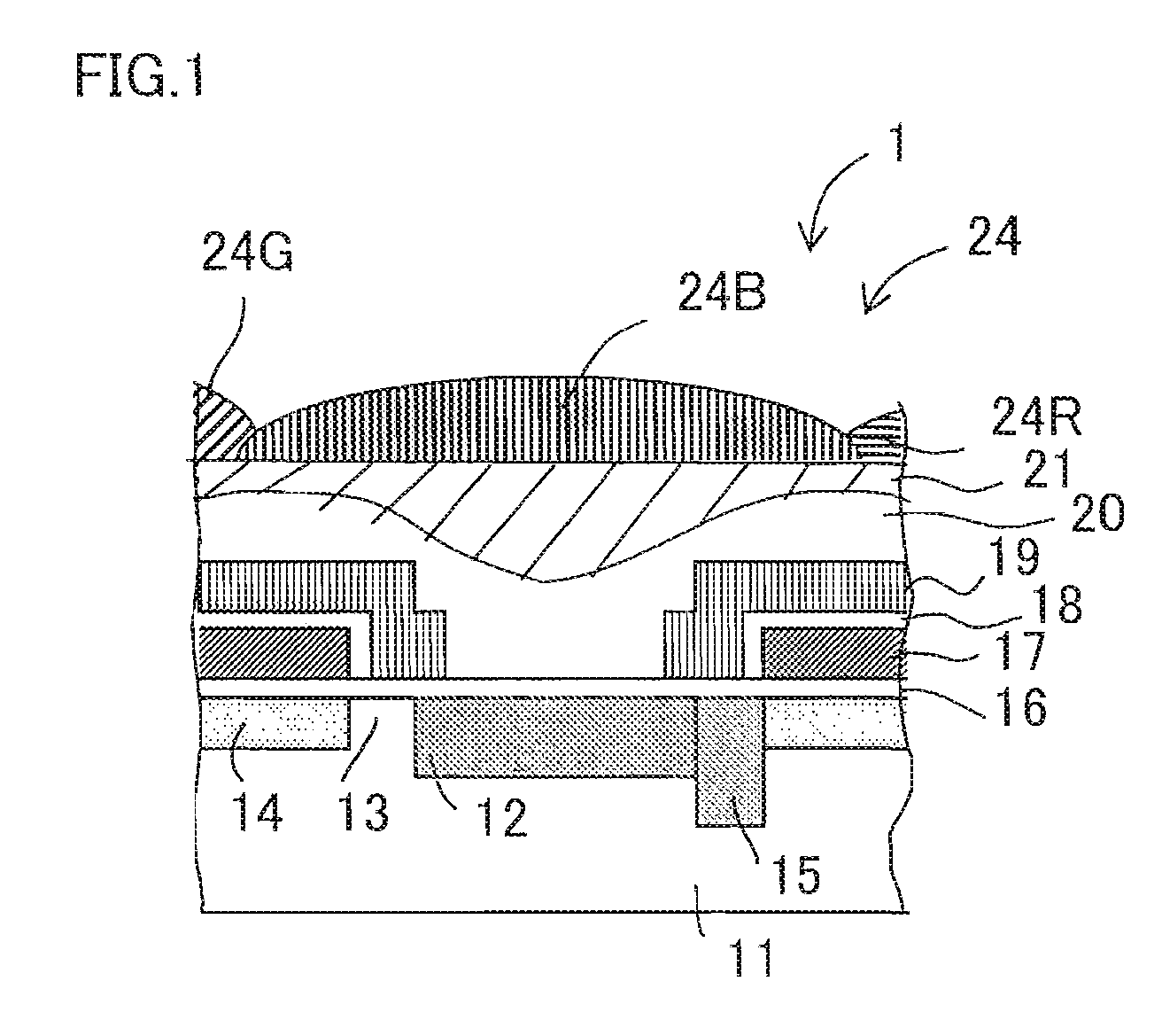
[0097]FIG. 1 is a longitudinal cross sectional view schematically illustrating an exemplary one-pixel structure in the CCD solid-state image capturing device of Embodiment 1 that uses the colored microlens array according to the present invention.

[0098]In FIG. 1, a CCD solid-state image capturing device 1 according to Embodiment 1 includes a plurality of light receiving sections 12 provided in a matrix on a surface of a semiconductor substrate 11, the light receiving sections 12 functioning as a plurality of photoelectric conversions section for performing photoelectric conversions on and capturing image light from a subject. A CCD charge transfer channel 14 is provided adjacent to the light receiving section 12 with a readout section 13 interposed therebetween, the CCD charge transfer channel 14 functioning to read out a signal charge from the light receiving section 12 through the readout section 13 and consecutively transfer the signal charge in a predetermined direction (either ...

embodiment 2

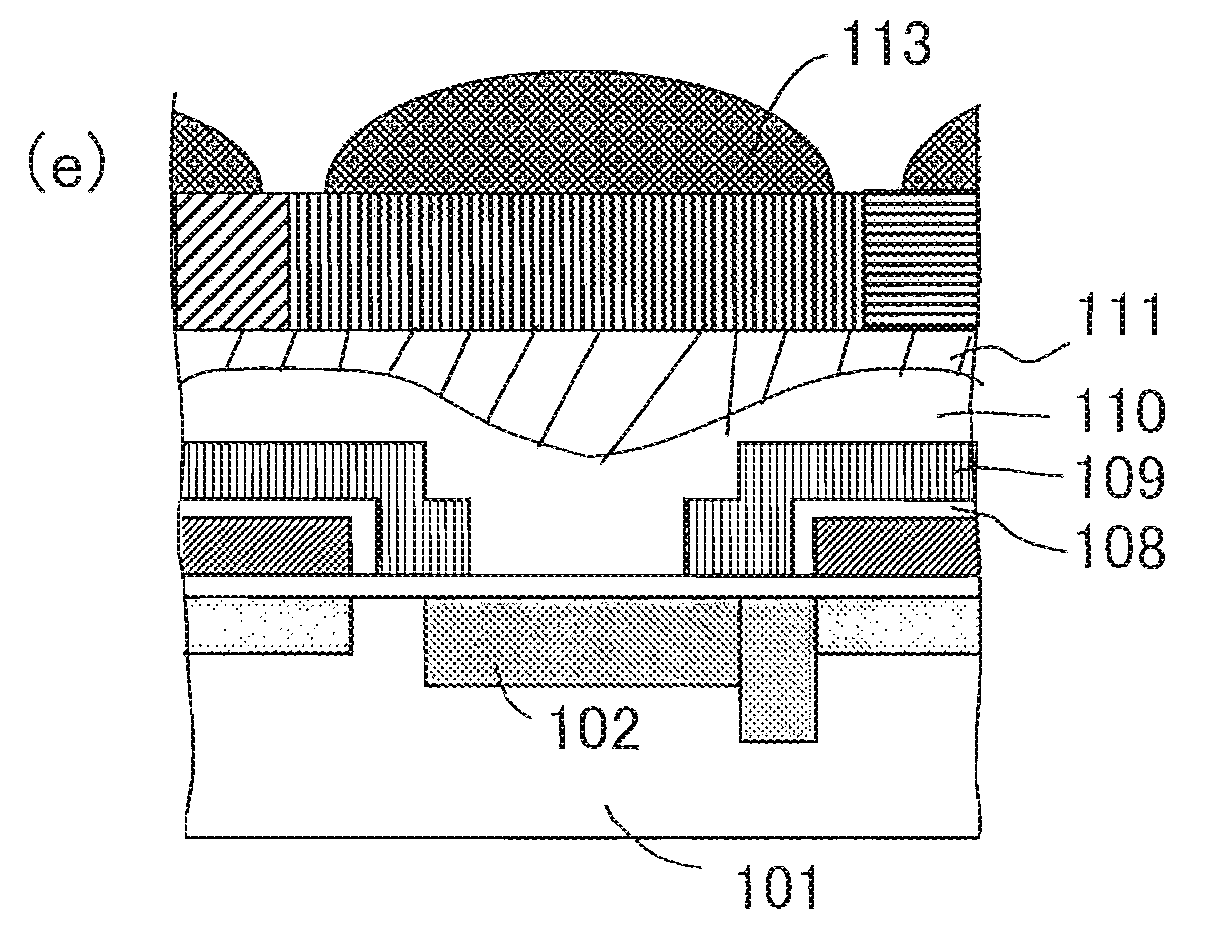
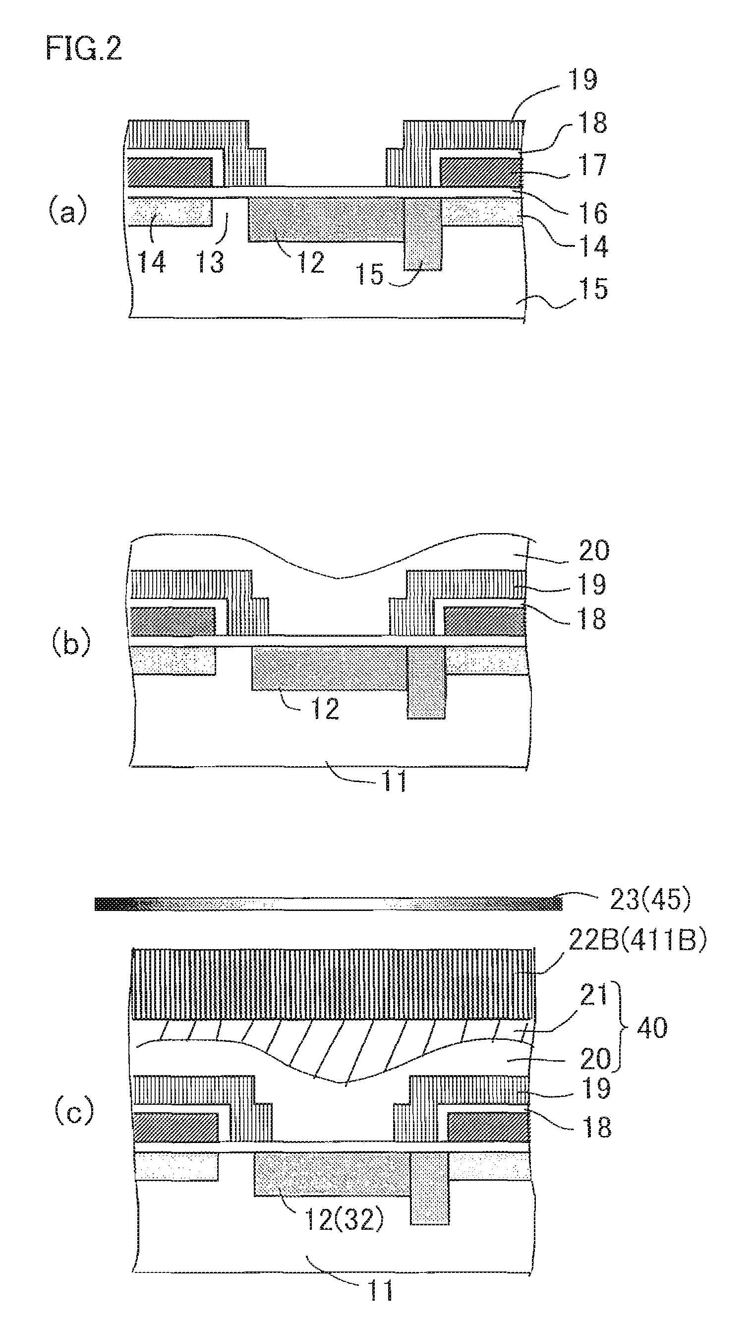
[0108]The colored microlens array according to the present invention and the manufacturing method for the colored microlens array has been described in Embodiment 1. In Embodiment 2, a case will be described where the colored microlens array according to the present invention and the manufacturing method for the colored microlens array are applied for an inner-layer lens. That is, in Embodiment 2, a case will be described where each surface of a plurality of microlenses is an inner-layer microlens provided inside a transparent film.

[0109]FIG. 5(a) is a longitudinal cross sectional view schematically illustrating an exemplary unit pixel structure of a CCD solid-state image capturing device equipped with an inner-layer microlens formed by a conventional method. FIG. 5(b) is a longitudinal cross sectional view schematically illustrating an exemplary unit pixel structure of a CCD solid-state image capturing device equipped with an inner-layer colored microlens formed in Embodiment 2 of ...

embodiment 3

[0119]In Embodiments 1 and 2, a case has been described where the colored microlens array according to the present invention and the manufacturing method for the colored microlens array are applied to a CCD solid-state image capturing device (CCD image sensor). In Embodiment 3, a case will be described where the colored microlens array according to the present invention and the manufacturing method for the colored microlens array are applied to a CMOS solid-state image capturing device (CMOS image sensor).

[0120]FIG. 6 is a longitudinal cross sectional view schematically illustrating an exemplary two-pixel structure in a CMOS solid-state image capturing device using a colored microlens array according to Embodiment 3 of the present invention.

[0121]In FIG. 6, a CMOS solid-state image capturing device 3 according to Embodiment 3 includes a P-type well region 52 formed on an N-type substrate 51, alight receiving section 53, which is composed of an N-type region, for forming a photodiode...


PUM


Abstract

A colored microlens array includes a plurality of microlenses for focusing incident light on a plurality of respective positions, on a substrate or a transparent film provided on the substrate, in which peripheral sections of the plurality of microlenses overlap each other at the adjacent positions and the microlenses are colored in a plurality of colors and arranged in a predetermined color arrangement.

Description

[0001]This Nonprovisional application claims priority under 35 U.S.C. §119(a) on Patent Application No. 2007-230842 filed in Japan on September 5, 2007, the entire contents of which are hereby incorporated by reference.BACKGROUND OF THE INVENTION[0002]1. Field of the Invention[0003]The present invention relates to a colored microlens array for focusing incident light at a plurality of positions by a predetermined color arrangement such as Bayer arrangement and a manufacturing method for the colored microlens array. In particular, the present invention relates to a colored microlens array for a colored microlens and an inner-layer lens used for a color solid-state image capturing apparatus consisting of semiconductor elements for performing photoelectric conversions on and capturing image light from a subject, used for a color liquid crystal display apparatus, and a manufacturing method for the colored microlens array; a color solid-state image capturing device using the colored micr...

Claims


Application Information

Patent Timeline
IPC IPC(8): H01L31/0232G02B27/10H01L31/18B29D11/00G02B3/00H01L27/14H04N5/335H04N5/369H04N9/07H04N101/00
CPCG02B3/0012H01L27/14685H01L27/14627G02B5/201
Inventor NAKAI, JUNICHI
Owner SHARP KK
Why Eureka
Try Eureka