Binocular Optical Relay Device

a technology of optical relay and binoculars, applied in the field of optics, can solve the problems of not being able to view sharp images at a closer distance, heavy crt display, bulky and not easily miniaturized, etc., and achieve the effect of reducing optical cross-talk

Inactive Publication Date: 2009-05-21
MIRAGE INNOVATIONS
View PDF70 Cites 98 Cited by
  • Summary
  • Abstract
  • Description
  • Claims
  • Application Information

AI Technical Summary

Benefits of technology

[0027]According to further features in preferred embodiments of the invention described below, the method further comprises attaching an additional optical element

Problems solved by technology

Unless a person is long-sighted, he may not be able to view a sharp image at a closer distance.
The CRT displays are heavy, bulky and not easily miniaturized.
The active matrix panel uses a transistor to control each pixel, and is more expensive.
Small size real image displays have a relatively small surface area on which to present a real image, thus have limited capability for providing sufficient information to the user.
In other words, because of the limited resolution of the human eye, the amount of details resolved from a small size real image might be insufficient.
For example, such displays have suffered from being too heavy for comfortable use, as well as too large so as to be obtrusive, distracting and even disorienting.
These defects stem from, inter alia, the incorporation of relatively large optics systems within the mounting structures, as well as physical designs which fail to adequately take into account important factors as size, shape, weight, etc.
A common problem to all types of holographic optical elements is their relatively high chromatic dispersion.
This is a major drawback in applications where the light source is not purely monochromatic.
Another drawback of some of these displays is the lack of coherence between the geometry of the image and the geometry of the holographic optical element, which c

Method used


Image

  • Binocular Optical Relay Device
  • Binocular Optical Relay Device
  • Binocular Optical Relay Device

Examples


example 1

Diffraction of Red Light

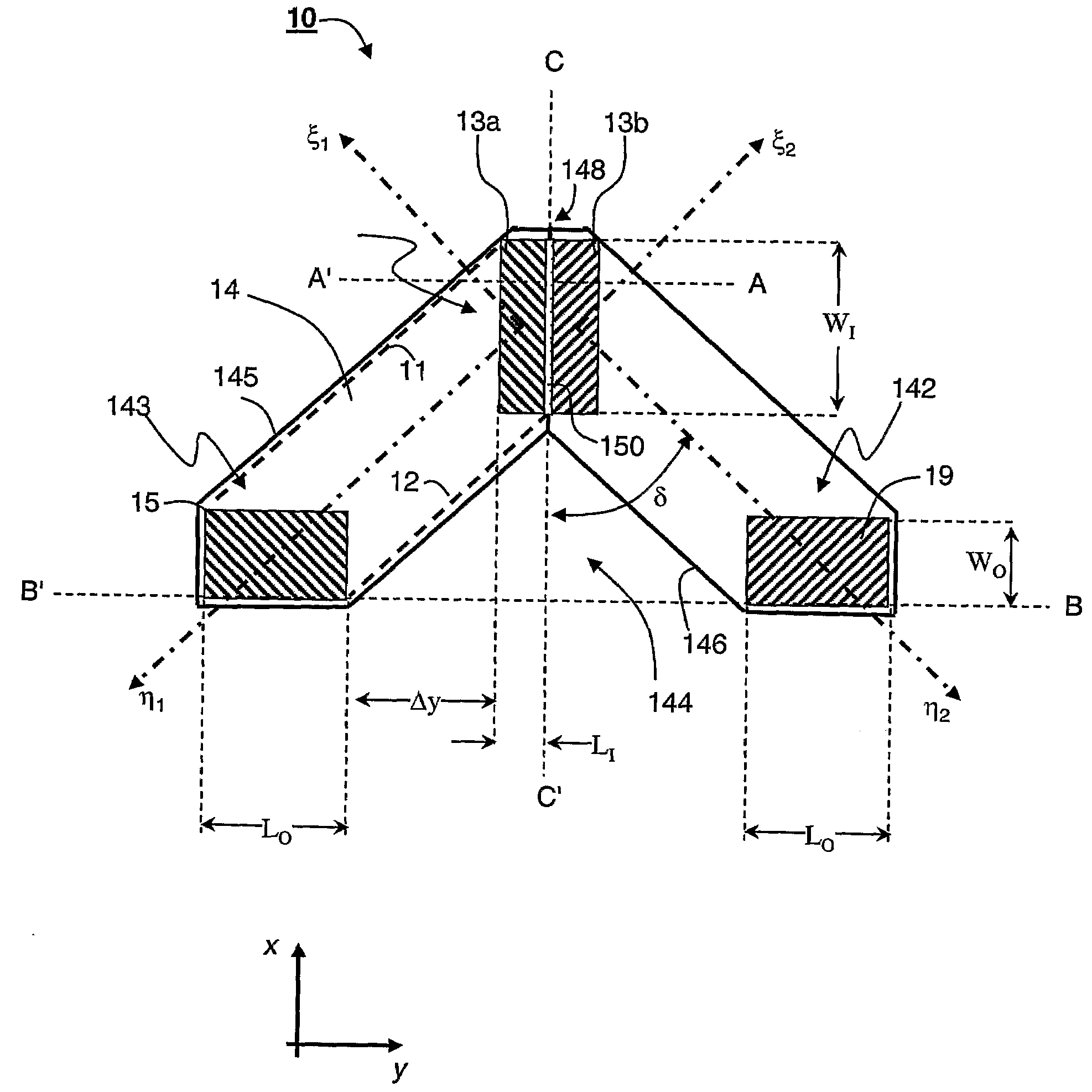
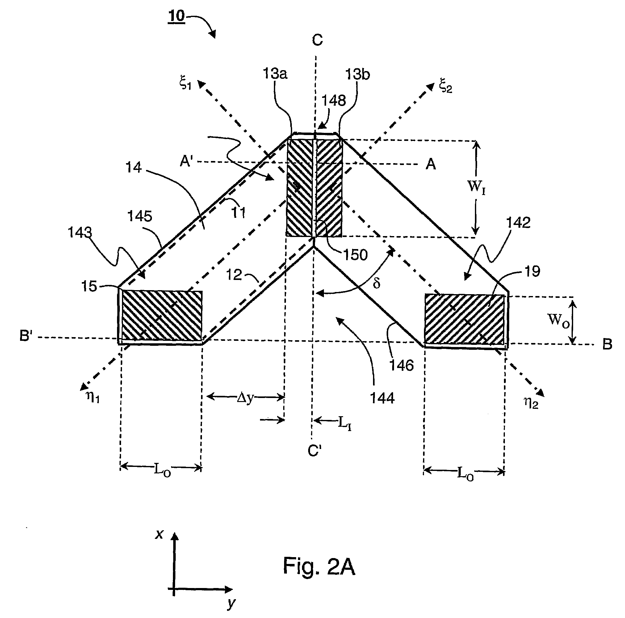
[0264]Following is a non-limiting example in which planar dimension calculations are performed in accordance with the teachings of the preferred embodiments of the invention for the diffraction of red light.

[0265]The present calculations are for 509 nm period gratings formed in a light transmissive substrate having index of refraction of 1.522, thickness of 2 mm, and apex angle of δ=62°. As a representative example for red light, a wavelength of 615 nm was assumed.

[0266]With the above values of the grating period, index of refraction and wavelength a horizontal field-of-view Ωy of [−12.0°, +12.0°] and a transverse field-of-view Ωx of [−9.0°, +9.0°] can be achieved. The overall (diagonal) field-of-view Ω is calculated using Equation 5 to obtain Ω=[−15°, +15°].

[0267]For Δz=25 mm, the minimal dimensions of the output optical element(s) are (see Equation 6) LO, min=10.6 mm and WO, min=7.9 mm. For LEB=4 mm, WEB=1 mm and Op=3 mm, the dimensions of the output optica...

example 2

Diffraction of Blue Light

[0271]Following is a non-limiting example in which planar dimension calculations are performed in accordance with the teachings of the preferred embodiments of the invention for the diffraction of blue light.

[0272]The present calculations are for 370 nm period gratings formed in a light transmissive substrate having index of refraction of 1.529, thickness of 1.8 mm, and apex angle of δ=60°. As a representative example for blue light, a wavelength of 465 nm was assumed.

[0273]With the above values of the grating period, index of refraction and wavelength a horizontal field-of-view Ωy of [−12°, +12°] and a transverse field-of-view Ωx of [−9°, +9°] can be achieved. The overall (diagonal) field-of-view Ω is calculated using Equation 5 to obtain Ω=[−15°, +15°].

[0274]For Δz=20 mm, the minimal dimensions of the output optical element(s) are LO, min=7.8 mm and WO,min=5.8 mm. For LEB=5 mm, WEB=2 mm and Op=3 mm the dimensions of the output optical element(s) are LO=15....

example 3

A Detailed Manufacturing Process

[0278]FIGS. 9A-L illustrate an exemplified embodiment for manufacturing the optical relay device according to the teachings of the present invention.

[0279]FIG. 9A schematically illustrates second substrate 218, which is preferably used for manufacturing the master substrate as further detailed hereinabove.

[0280]FIG. 9B schematically illustrates second substrate 218, once layer 220 of photoresist material is applied thereon.

[0281]FIG. 9C schematically illustrates second substrate 218, once pattern 222 is recorded on layer 220

[0282]FIG. 9D schematically illustrates second substrate 218, once the photoresist is developed to form mask pattern 224 on layer the surface of substrate 218.

[0283]FIG. 9E schematically illustrates substrate 218 following the etching process which forms the inverted shape 202 of the grating on substrate 218.

[0284]FIG. 9F schematically illustrates substrate 218 following once mask pattern 224 is removed.

[0285]FIG. 9G schematically ...


PUM


Abstract

An optical relay device, comprising a light-transmissive substrate shaped as a structure having an apex section, a right section and a left section being separated from the right section by an air gap. The optical relay device further comprises at least two input optical elements located at the apex section, a right output optical element located at the right section, and a left output optical element located at the left section. The substrate and the optical elements are designed and constructed such that light is redirected by the input optical elements, propagates via total internal reflection in the direction of at least one of the sections, and redirected out of the substrate by at least one output optical element.

Description

FIELD AND BACKGROUND OF THE INVENTION[0001]The present invention relates to optics, and, more particularly, to a binocular optical relay device and system capable of providing monochrome or multicolor images.[0002]Miniaturization of electronic devices has always been a continuing objective in the field of electronics. Electronic devices are often equipped with some form of a display, which is visible to a user. As these devices reduce in size, there is an increase need for manufacturing compact displays, which are compatible with small size electronic devices. Besides having small dimensions, such displays should not sacrifice image quality, and be available at low cost. By definition the above characteristics are conflicting and many attempts have been made to provide some balanced solution.[0003]An electronic display may provide a real image, the size of which is determined by the physical size of the display device, or a virtual image, the size of which may extend the dimensions ...

Claims


Application Information

Patent Timeline
IPC IPC(8): G02B23/04
CPCG02B5/1847G02B5/1866G02B6/0016G02B6/0038G02B2027/0132G02B27/0172G02B2027/011G02B2027/0125G02B27/0081
Inventor NIV, YEHUDABEKER, AMIR
Owner MIRAGE INNOVATIONS
Why Eureka
Try Eureka