Chip for analyzing a medium comprising an integrated organic light emitter

Inactive Publication Date: 2009-05-28
FRAUNHOFER GESELLSCHAFT ZUR FOERDERUNG DER ANGEWANDTEN FORSCHUNG EV
View PDF6 Cites 19 Cited by
  • Summary
  • Abstract
  • Description
  • Claims
  • Application Information

AI Technical Summary

Benefits of technology

[0032]Embodiments of the present invention further enable omission of color filters in the spectral selection of the detectors, and thus enable monitoring of the homogeneity of the illumination. Thus, embodiments allow a clear reduction in the chip area, a reduction in

Problems solved by technology

Hybrid integration of light emitter and light detector, for example in the form of connecting prefabricated devices, in principle entails a large fabrication effort and does not allow general price degression, especially with large numbers of pieces.
Furthermore, due to the hybrid structure, a desired level of reliability can only be achieved at extremely high cost.
Light-emitting diodes based on inorganic semiconductors exhibit significant disadvantages for many applications.
Since they are realized on monocrystalline substrates, they can only be applied to III-V semiconductor backgrounds or, if this is not possible, be mounted on an extraneous substrate, w

Method used


Image

  • Chip for analyzing a medium comprising an integrated organic light emitter
  • Chip for analyzing a medium comprising an integrated organic light emitter
  • Chip for analyzing a medium comprising an integrated organic light emitter

Examples


Embodiment Construction

[0043]Before the present invention will be explained below in more detail on the basis of the drawings, it shall be noted that identical elements in the figures are given identical or similar reference numerals, and that repeated descriptions of these elements shall be dispensed with.

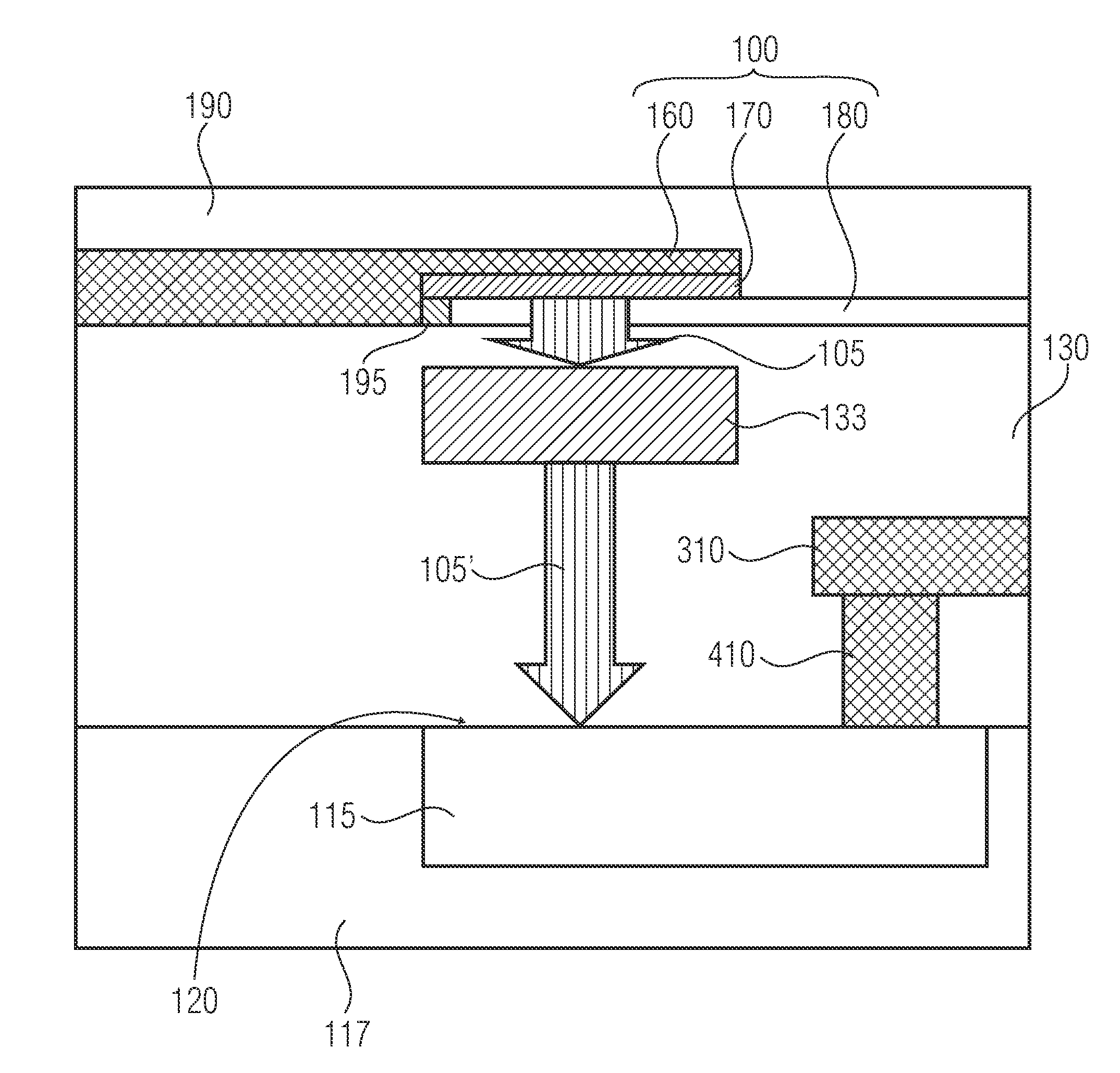
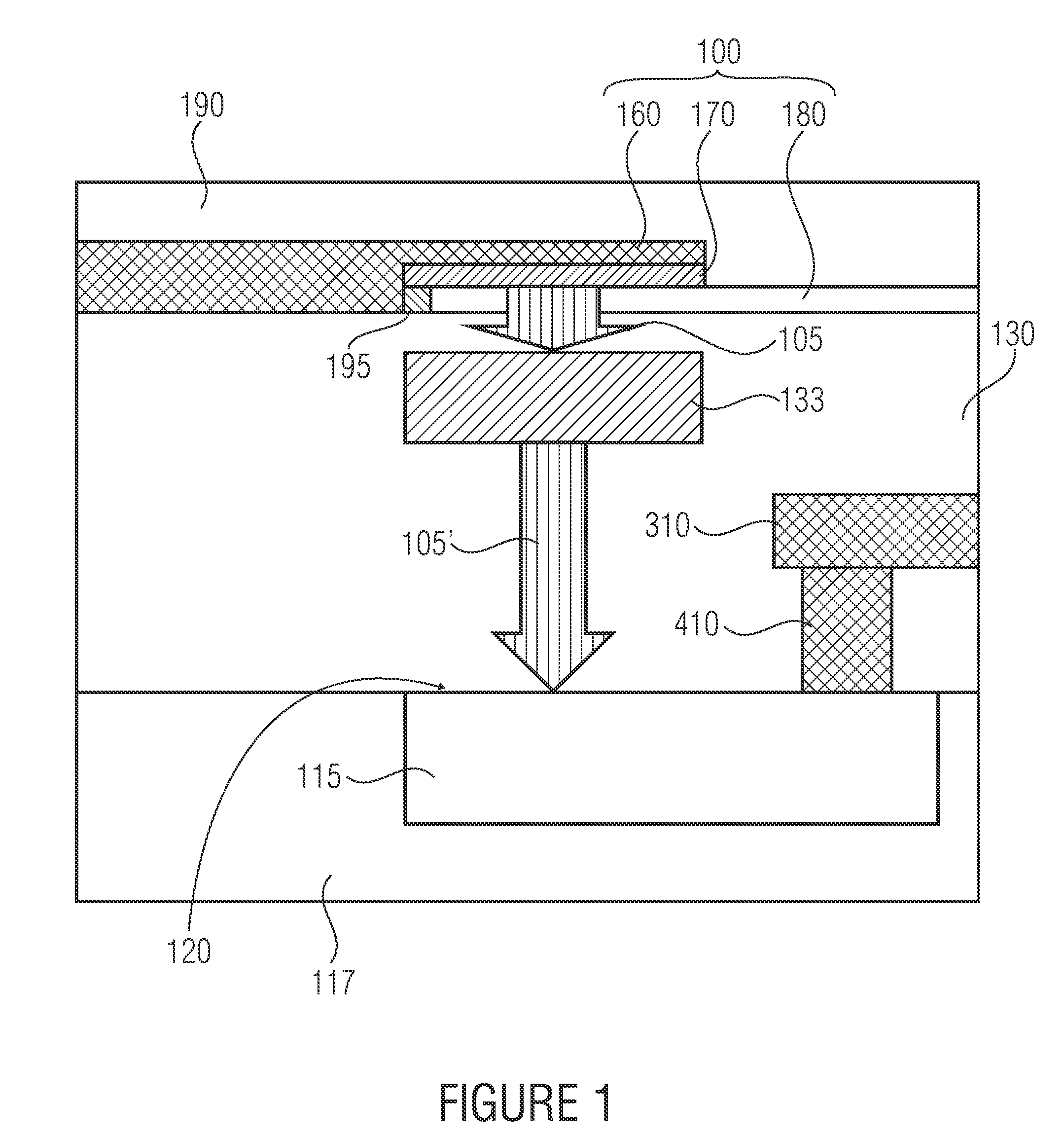
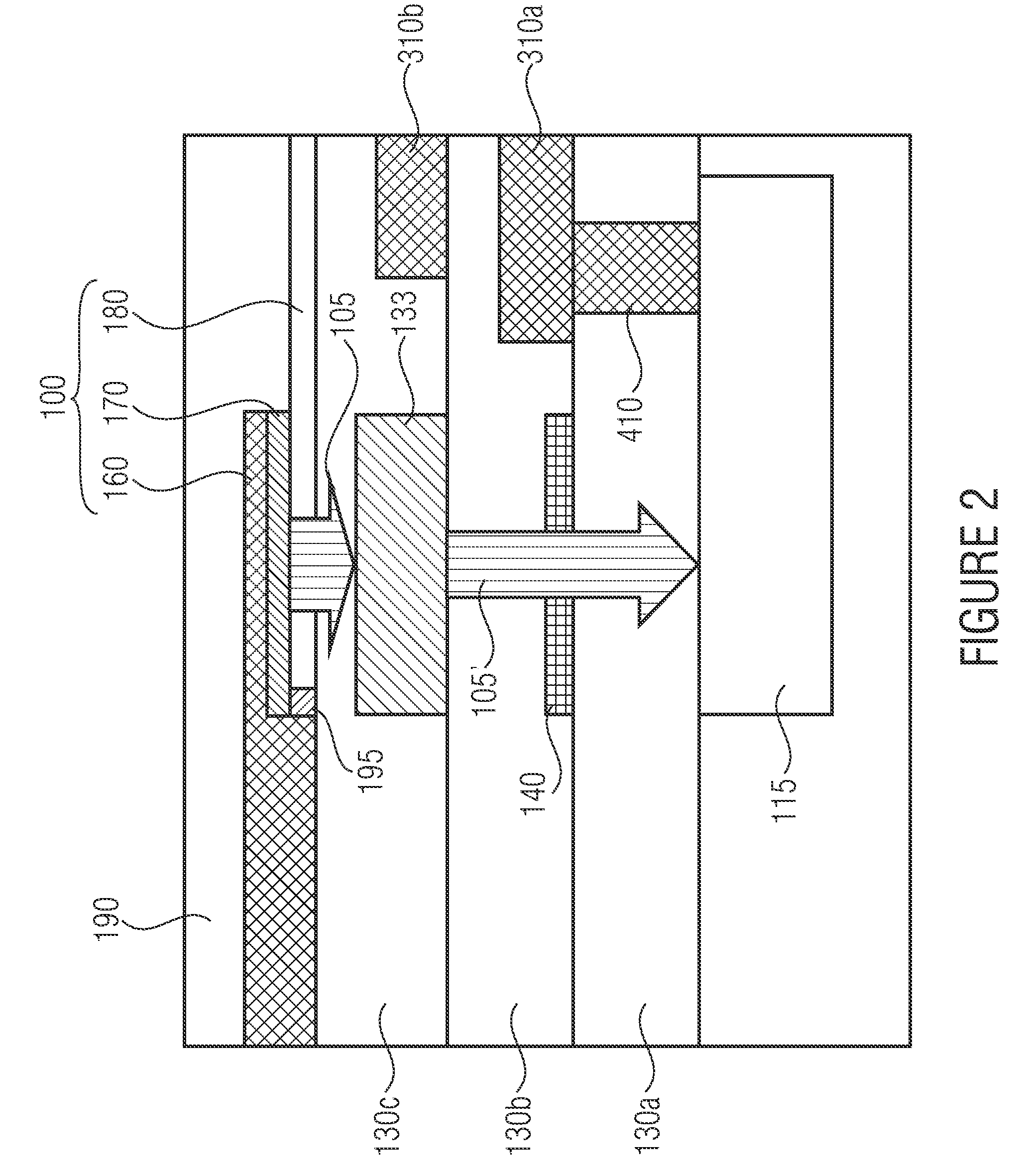
[0044]FIG. 1 shows an embodiment in which a photodetector comprises a photodiode 115 which may be formed, for example, by means of a pn junction of an n well to a substrate 117 or to a p+-doped surface layer (or which uses any other existing pn junction). The photodiode 115 comprises a detector area 120 and is contacted with a shielding plane 310 via the contact 410. Further contacts of the photodetector are not depicted for simplicity's sake. The photodetector 115 and the OLED 100 are separated by a layer sequence 130 comprising a reservoir 133. The reservoir 133 may be implemented as a reagent reservoir or microchannel, and may serve as a container for the medium (e.g. serum) to be examined. It may th...


PUM


Abstract

A chip for analyzing a medium includes an organic light emitter for emitting a light signal, a photodetector including a detector area, a layer sequence separating the organic light emitter and the detector area, and a reservoir into which the medium may be introduced. The organic light emitter and the photodetector are optically couplable by means of a path of rays of the light signal, and the reservoir is arranged within the path of rays of the light signal.

Description

CROSS-REFERENCE TO RELATED APPLICATIONS:[0001]This application claims priority from German Patent Application No. 102007056275.8, which was filed on Nov. 22, 2007, and is incorporated herein by reference in its entirety.[0002]The present invention relates to a chip for analyzing a medium comprising an integrated organic light emitter, and in particular to a monolithically integrated lab-on-chip device comprising an OLED light source (OLED=organic light-emitting diode).BACKGROUND OF THE INVENTION[0003]Nowadays, microarrays are widely used in medical diagnostics. They comprise, for example, realizing a grid-shaped arrangement (array or matrix arrangement) of small containers or pots, into which biologically active substances (the medium) may be introduced, on a surface. For example, the array may be wetted or covered with a serum such as blood, so that it is possible to examine how sought-for substances from the serum are fixed within the various pots of the array. At the same time, t...

Claims


Application Information

Patent Timeline
IPC IPC(8): G01J1/20
CPCB01L3/5027B01L3/502707G01N21/6408G01N2201/0627G01N2021/7789G01N2201/062G01N21/6454G01N21/31G01J3/10G01J3/4406G01J3/0259
Inventor LEO, KARLVOGEL, UWE
Owner FRAUNHOFER GESELLSCHAFT ZUR FOERDERUNG DER ANGEWANDTEN FORSCHUNG EV
Why Eureka
Try Eureka