Unlock instant, AI-driven research and patent intelligence for your innovation.

System and Method for Scanning Sequential Logic Elements

a logic element and sequential logic technology, applied in the field of digital systems, can solve the problems of ic improper function, increased complexity of modern integrated circuitry, and increased likelihood of at least one transistor contained on the ic malfunctioning after fabrication,

Inactive Publication Date: 2009-05-28
LENOVO GLOBAL TECH INT LTD
View PDF10 Cites 6 Cited by
  • Summary
  • Abstract
  • Description
  • Claims
  • Application Information

AI Technical Summary

Benefits of technology

"The patent describes a power-saving solution for digital systems that allows for chip testing. The solution involves dividing sequential logic elements into power domains, with one or more power domains being power gated. A scan chain is used to process a scan data sequence, and a scan enable switch controls a scan mode. A shadow engine with a control circuit can override the scan data sequence for a number of times to allow for constant value insertion. The method also includes bypassing the power gated power domain with a sequence of sequential logic elements using the shadow engine. The technical effects of this solution include reducing power consumption and improving testing efficiency."

Problems solved by technology

The complexity of modern integrated circuitry continues to increase at a dramatic rate.
However, with the increase in transistor numbers on each IC, the likelihood that at least one transistor contained on the IC malfunctions after fabrication also increases.
When the outputs fail to correctly correspond to the expected results, the IC has improperly functioned.
When the output is not the correct output when designing the IC, a diagnostic engineer still must spend a significantly large amount of time identifying which malfunctioning transistor or set of malfunctioning transistors caused the error.
Thus, in modern ICs, the ability to test internal logic with standard functional or operational vectors is no longer cost efficient.
The transistor-to-package pin ratio is typically too large to successfully verify the internal structure of the chip in a reasonable amount of vectors or test time.
Furthermore, many techniques that have been used to test and verify densely packed board designs cannot be used within the operation of the IC, because there is no direct access to many of the circuits within the packaged and sealed IC.
Due to the fact that modern semiconductor chips, especially processor chips, comprise a plurality of electronic elements, one is also faced with the problem of very high power consumption.
If such a power domain is switched off or if the circuit's voltage is reduced, then a scanning process is not possible on the power domain, since the logic inside the power domain is not functional.
Hence, the entire scan chain is interrupted, and it is no longer possible to scan the storage elements on the active power domains of the semiconductor chip.
However, such technique results in a huge power consumption peak that may be not be supported currently by the system.
Moreover, the activation of all power domains for scanning purposes takes a relatively long time.
However, such technique requires additional wires running from and to the scan engine.
Thus, the complexity of the scan structure and its verification is increased.
Moreover, such solution requires a change to the chip masks and a remanufacturing of the semiconductor chip.
Furthermore, in this solution the user must activate the power domain to be scanned beforehand, and more overhead must be added to the software.
However, the drawback of such approach is the creation of scan patterns of varying length depending on the current power gating status.
However, read-out circuitry would have to adapt to a large variety of possible scan chain lengths, and currently chip tests do not support state-dependent scan chain lengths.

Method used


Image

  • System and Method for Scanning Sequential Logic Elements
  • System and Method for Scanning Sequential Logic Elements
  • System and Method for Scanning Sequential Logic Elements

Examples


Embodiment Construction

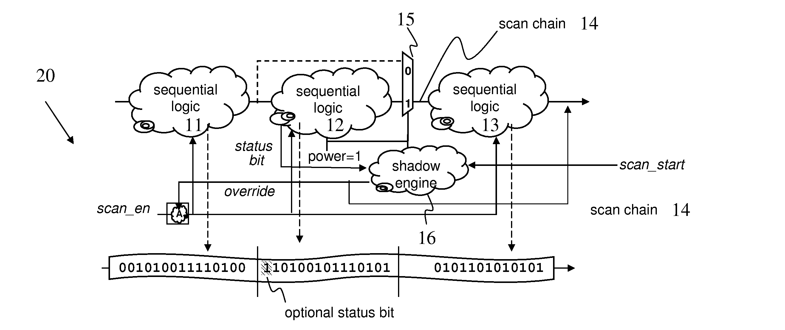
[0028]It is already well known to bypass a power gated power domain of a digital system. The use of a bypass permits circumvention of the drawback from power gated domains when scan testing the digital system. FIG. 1A and FIG. 1B illustrate three power domains 1, 2, and 3, each comprising sequential logic elements (e.g., latches), of a digital system 10 according to the prior art. The power domains 1, 2, and 3 are interconnected to a scan chain 4. The power domain 2 can be bypassed by using a multiplexer 5 to the scan chain 4 to bridge the power gated portions within the scan chain 4. A power indication signal is used to facilitate such power gating; such signal indicates either “power=1” (when the power domain 2 is not power gated as in FIG. 1A) or “power=0” (when the power domain 2 is power gated as in FIG. 1B). When the power domain 2 is power gated (FIG. 1B), it is bypassed during scan testing. Consequently, the corresponding scan chain 4 comprises only scan testing information ...


PUM


Abstract

System and Method for Scanning Sequential Logic Elements A digital system and method for scanning sequential logic elements are disclosed. The digital system may comprise a plurality of sequential logic elements subdivided into power domains, wherein at least one of the power domains is power gated; a scan chain configured for processing a scan data sequence; a scan enable switch configured for controlling a scan mode; and at least one shadow engine, wherein the at least one shadow engine comprises a control circuit. At least some of the power domains may be interconnected to the scan chain with the scan enable switch, and the scan enable switch may control the scan mode by asserting a scan enable signal. The at least one power gated power domain with one or more sequential logic elements to be power gated may be bypassed via the at least one shadow engine.

Description

RELATED APPLICATION[0001]This application claims priority under 35 U.S.C. §119 to European Patent Application No. 07121266.6 filed Nov. 22, 2007, the entire text of which is specifically incorporated by reference herein.TECHNICAL FIELD[0002]The various embodiments described herein relate to a digital system comprising a plurality of sequential logic elements subdivided into power domains, wherein at least some of the power domains with sequential logic elements are interconnected to a scan chain with a scan enable switch. During scan mode, scanning data is loaded or unloaded to be transferred from one sequential logic element to another in order to be scanned on each clock pulse when a scan enable signal is asserted. Furthermore, the various embodiments relate to a method for scanning sequential logic elements of such digital system.BACKGROUND OF THE INVENTION[0003]The complexity of modern integrated circuitry continues to increase at a dramatic rate. Modern integrated circuits (ICs...

Claims


Application Information

Patent Timeline
Patent Type & Authority Applications(United States)
IPC IPC(8): H04L27/06
CPCG01R31/318536
Inventor GEMMEKE, TOBIASWENDEL, DIETERWETTER, HOLGERLEENSTRA, JENS
Owner LENOVO GLOBAL TECH INT LTD