Methods for nanopatterning and production of magnetic nanostructures
- Summary
- Abstract
- Description
- Claims
- Application Information
AI Technical Summary
Benefits of technology
Problems solved by technology
Method used
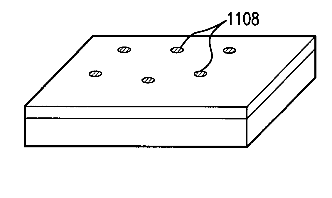
Image

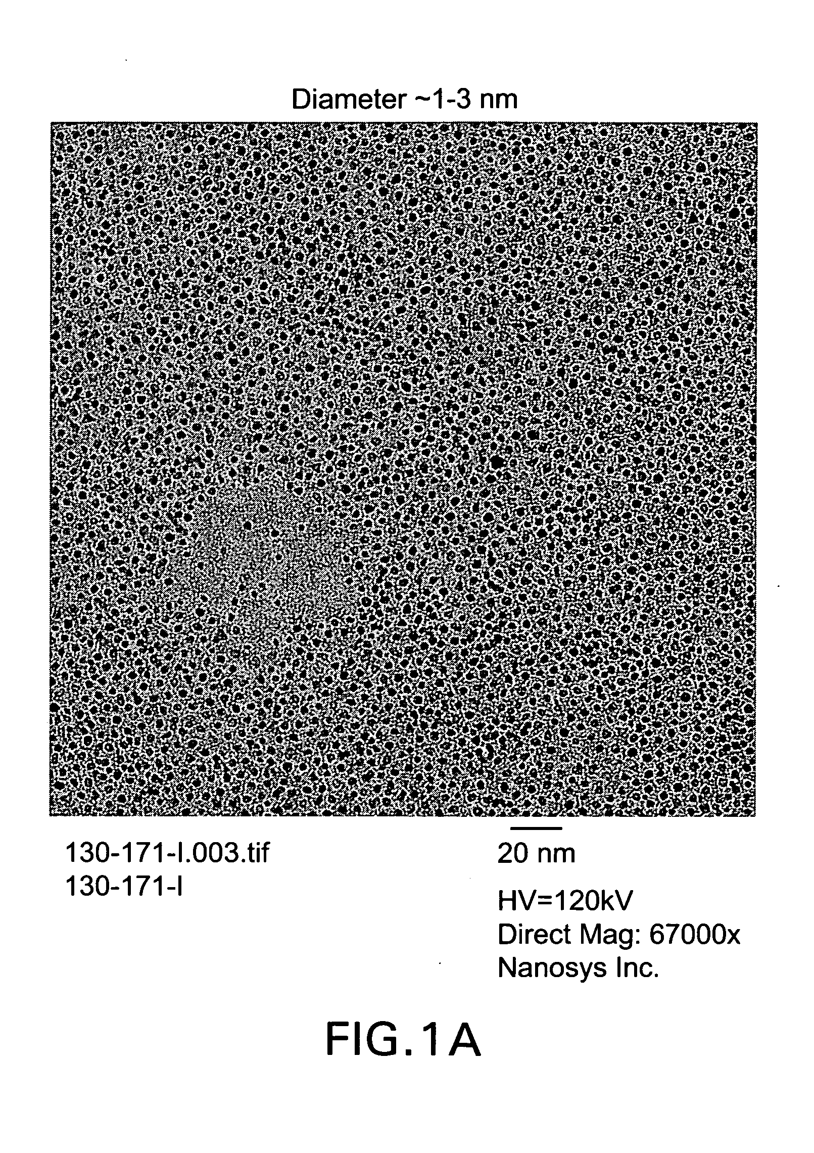
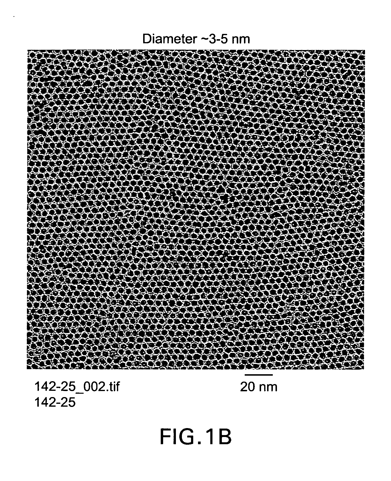
Examples
Embodiment Construction
[0033]It should be appreciated that the particular implementations shown and described herein are examples of the invention and are not intended to otherwise limit the scope of the present invention in any way. Indeed, for the sake of brevity, conventional electronics, manufacturing, semiconductor devices, and nanocrystal, nanoparticle, nanowire (NW), nanorod, nanotube, and nanoribbon technologies and other functional aspects of the systems (and components of the individual operating components of the systems) may not be described in detail herein. Further, the techniques are suitable for applications in electrical systems, optical systems, consumer electronics, industrial or military electronics, wireless systems, space applications, or any other application.
[0034]As used herein, the term “nanostructure” refers to a structure that has at least one region or characteristic dimension with a dimension of less than about 500 nm, including on the order of less than about 1 nm. As used h...
PUM
 Abstract
Description
Claims
Application Information