High Temperature Interfacial Superconductivity

a superconductivity and high temperature technology, applied in the field of interfacial superconductivity, can solve the problems of conflicting challenges in the ale of hts materials, limited success in the development of commercially viable electronic devices and integrated circuits which utilize hts materials, and enhanced interdiffusion at film interfaces, so as to achieve heightened superconducting transition temperatures

Inactive Publication Date: 2009-05-28
BROOKHAVEN SCI ASSOCS
View PDF24 Cites 26 Cited by
  • Summary
  • Abstract
  • Description
  • Claims
  • Application Information

AI Technical Summary

Benefits of technology

[0014]In view of the above-described problems and goals, it is an objective of the present invention to provide uniform, ultrathin, and stable superconducting interfacial layers with heightened superconducting transition temperatures. In one embodiment, interfacial superconductivity occurs due to charge depletion and accumulation across an interface between two materials which may not themselves be superconducting due to differences in the chemical potential of the two layers forming the superconducting interface. This may be accomplished, for example, by sequentially depositing a thin layer of an electrically conducting material (M) and an electrically insulating material (I), both of which are not themselves superconducting. The deposition process is controlled with atomic-level precision such that the transition between successive M-I layers is atomically abrupt. The interface between the two materials exhibits superconducting behavior, irrespective of the order (M-I or I-M) in which they are deposited. The superconductivity originates from and is confined to a few unit cells surrounding the interface, being preferably confined to ≦2 unit cells. The M and I layers are preferably ≧5 unit cells thick, but are not so limited. The form of M and I is not limited to thin layers, but may be any form, shape, or structure which permits a superconducting interface to be formed between them.

Problems solved by technology

Despite advances in the ALE of HTS, the development of commercially viable electronic devices and integrated circuits which utilize HTS materials has been met with limited success.
Although HTS-based electronic devices show great promise with the potential to realize very high switching speeds with minimal power consumption and negligible thermal losses, actual fabrication of such devices requires solutions to a number of challenging materials-related problems.
These requirements pose conflicting challenges for the ALE of HTS materials.
High growth temperatures are generally required to ensure excellent crystallinity; however, higher temperatures may also lead to surface roughening and enhanced interdiffusion at film interfaces.
Thus far, it has proved very difficult to achieve bulk Tc values in very thin HTS films; the transitions are typically broad and the Tc is low.
Another problem encountered with ultrathin HTS materials is that subsequent processing steps necessary to fabricate actual electronic devices tend to degrade the material quality.
Additional materials challenges which have hindered the development of HTS layers include improvements in film quality and reproducibility over large areas and between different deposition sequences, but under identical deposition conditions.
In addition to the problems associated with fabrication of suitable HTS materials, there is a continuing and ever-present need to produce superconductors with still higher Tc.

Method used


Image

  • High Temperature Interfacial Superconductivity
  • High Temperature Interfacial Superconductivity
  • High Temperature Interfacial Superconductivity

Examples


Embodiment Construction

[0041]The above and other objectives of the invention will become more apparent from the following description and illustrative embodiments which are described in detail with reference to the accompanying drawings. Similar elements in each figure are designated by like reference numbers and, hence, subsequent detailed descriptions thereof may be omitted for brevity. In the interest of clarity, the following terms and acronyms are defined as provided below.

DEFINITIONS

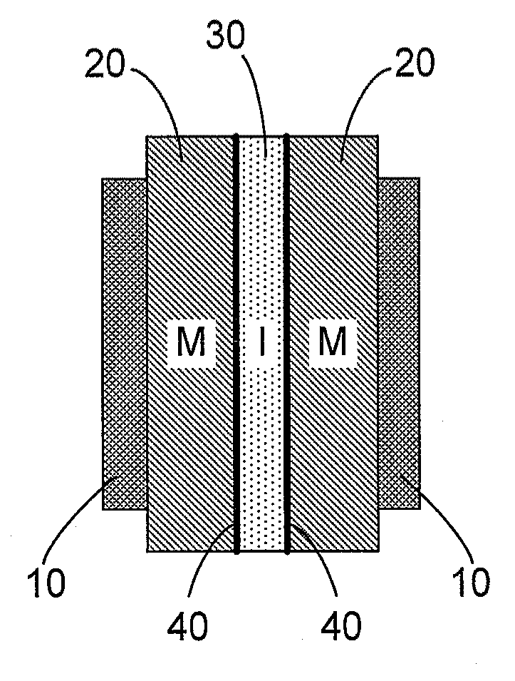
[0042]Adatom: An atom located on the surface of an underlying substrate.[0043]Atomically Sharp Generally used to characterize a transition from one material to another. When a transition from one layer to another is atomically sharp, the transition occurs abruptly on an atomic scale. This means that there is no concentration gradient or gradual transition between the two layers. Atomically abrupt is synonymous with atomically sharp.[0044]Bilayer: Two layers of different materials with arbitrary thicknesses which are stac...


PUM

PropertyMeasurementUnit
surface roughnessaaaaaaaaaa
Tcaaaaaaaaaa

Abstract

High-temperature superconductivity confined to nanometer-scale interfaces has been a long standing goal because of potential applications in electronic devices. The spontaneous formation of a superconducting interface in bilayers consisting of an insulator (La2CuO4) and a metal (La1−xSrxCuO4), neither of which is superconducting per se, is described. Depending upon the layering sequence of the bilayers, Tc may be either ˜15 K or ˜30 K. This highly robust phenomenon is confined to within 2-3 nm around the interface. After exposing the bilayer to ozone, Tc exceeds 50 K and this enhanced superconductivity is also shown to originate from a 1 to 2 unit cell thick interfacial layer. The results demonstrate that engineering artificial heterostructures provides a novel, unconventional way to fabricate stable, quasi two-dimensional high Tc phases and to significantly enhance superconducting properties in other superconductors. The superconducting interface may be implemented, for example, in SIS tunnel junctions or a SuFET.

Description

CROSS-REFERENCE TO RELATED APPLICATIONS[0001]This application claims priority to U.S. Provisional Patent Application No. 60 / 986,186 filed on Nov. 7, 2007 under 35 U.S.C. § 119(e), the entirety of which is incorporated by reference as if fully set forth in this specification.STATEMENT OF GOVERNMENT LICENSE RIGHTS[0002]The present invention was made with government support under contract number DE-AC02-98CH10886 awarded by the U.S. Department of Energy. The United States government has certain rights in the invention.BACKGROUND OF THE INVENTION[0003]I. Field of the Invention[0004]This invention relates generally to interfacial superconductivity. In particular, the present invention relates to the formation of an ultrathin and stable superconducting layer at the interface between two materials. This invention further relates to the utilization of such a superconducting interface in electronic devices.[0005]II. Background of the Related Art[0006]The discovery of a class of copper-oxide ...

Claims


Application Information

Patent Timeline
Patent Type & Authority Applications(United States)
IPC IPC(8): H01L39/02H01L39/24
CPCH01L39/128H01L39/2432H01L39/225H01L39/146Y10T428/31678H10N60/858H10N60/207H10N60/124H10N60/0381
Inventor BOZOVIC, IVANLOGVENOV, GENNADYGOZAR, ADRIAN MIHAI
Owner BROOKHAVEN SCI ASSOCS
Why Eureka
Try Eureka