Bolometer and method of manufacturing the same

a technology of bolometer and insulating layer, which is applied in the field of bolometer, can solve the problems of not being able to directly deposit a single crystalline silicon thin film on a substrate, and achieve the effects of reducing noise, high crystallinity, and increasing temperature sensitivity

Inactive Publication Date: 2009-06-04
ELECTRONICS & TELECOMM RES INST
View PDF15 Cites 36 Cited by
  • Summary
  • Abstract
  • Description
  • Claims
  • Application Information

AI Technical Summary

Benefits of technology

[0018]The present invention is directed to a bolometer and a method of manufacturing the same, the bolometer having reduced noise and increas

Problems solved by technology

However, it is impossible to directly deposit a single crystalline silicon thin film on a substrate

Method used


Image

  • Bolometer and method of manufacturing the same
  • Bolometer and method of manufacturing the same
  • Bolometer and method of manufacturing the same

Examples


Embodiment Construction

[0026]Hereinafter, the present invention will be described in detail with reference to the accompanying drawings. This invention may, however, be embodied in different forms and should not be construed as limited to the embodiments set forth herein. Rather, these embodiments are provided so that this disclosure will be thorough enough to enable those skilled in the art to embody and practice the invention. In the drawings, the thickness of layers and regions may be exaggerated for clarity and elements are consistently designated by the same reference numerals.

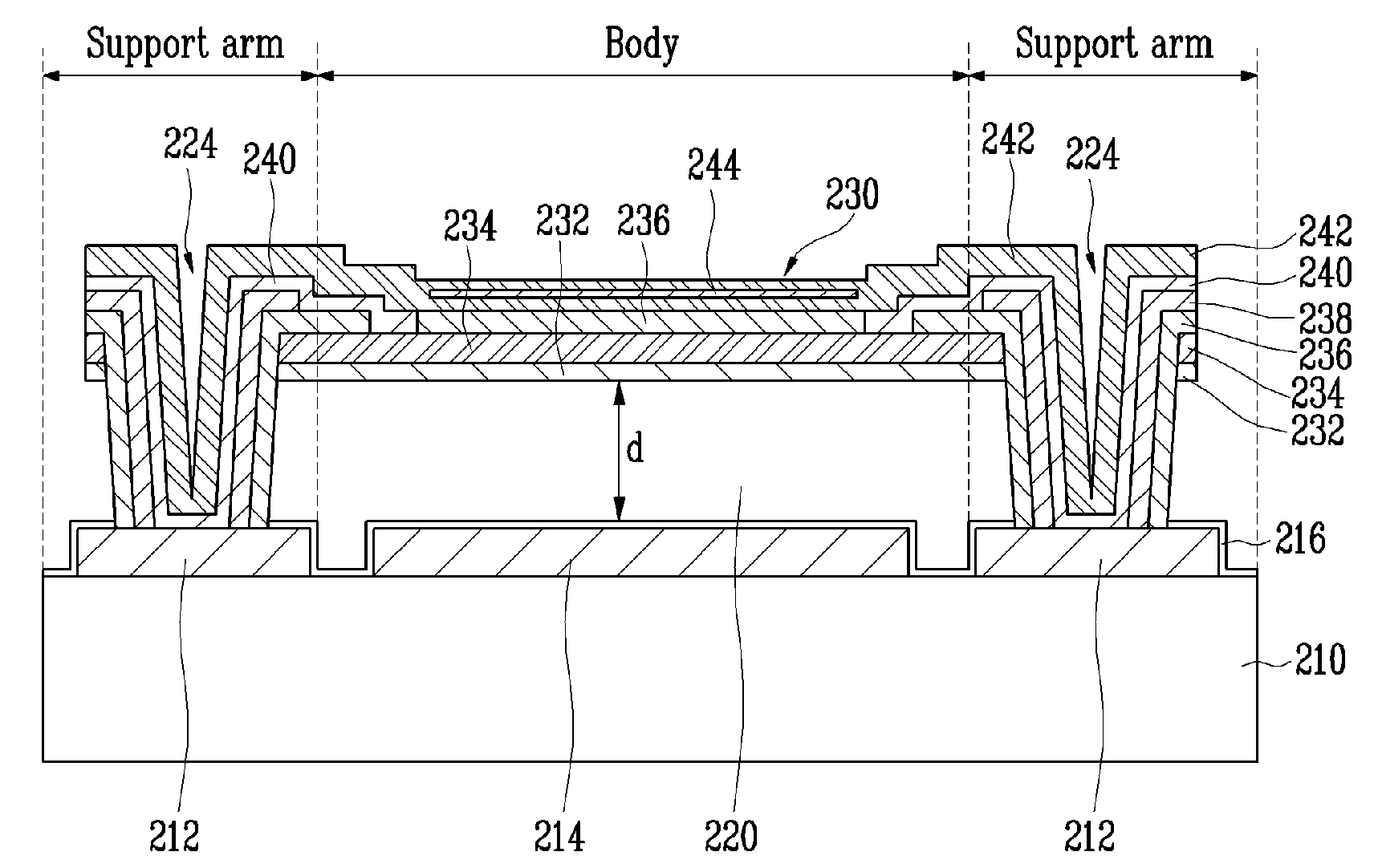
[0027]FIG. 2 illustrates a bolometer according to an exemplary embodiment of the present invention.

[0028]Referring to FIG. 2, the bolometer of the present invention includes a substrate 210 having a detecting circuit (not illustrated), a reflecting layer 214 formed at a predetermined part of the surface of the substrate 210, and a sensor structure 230 spaced an air-gap 220 of λ / 4 apart from the reflecting layer 214.

[0029]The se...


PUM


Abstract

A bolometer having decreased noise and increased temperature sensitivity and a method of manufacturing the same are provided. The bolometer has a resistive layer formed of single crystalline silicon (Si) or silicon germanium (Si1-xGex, x=0.2˜0.5) having high crystallinity, such that 1/f noise can be reduced and temperature sensitivity can be significantly improved compared to a conventional amorphous silicon bolometer.

Description

CROSS-REFERENCE TO RELATED APPLICATION[0001]This application claims priority to and the benefit of Korean Patent Application No. 2007-122577, filed Nov. 29, 2007, the disclosure of which is incorporated herein by reference in its entirety.BACKGROUND[0002]1. Field of the Invention[0003]The present invention relates to a bolometer and a method of manufacturing the same, and more particularly, to a bolometer in which a resistive layer is formed of single crystalline silicon (Si) or silicon germanium (Si1-xGex, x=0.2˜0.5) having high crystallinity to reduce noise and enhance temperature sensitivity, and a method of manufacturing the same.[0004]This work was supported by the IT R&D program of MIC / IITA [2006-S-054-02, Development of Ubiquitous CMOS-based MEMS multifunctional sensor].[0005]2. Discussion of Related Art[0006]Infrared sensors are classified into a cooled sensor operating at the temperature of liquid nitrogen, and a uncooled sensor operating at room temperature. The cooled inf...

Claims


Application Information

Patent Timeline
IPC IPC(8): H01L27/14H01L21/00
CPCG01J5/20H01L31/09
Inventor YANG, WOO SEOKCHO, SEONG MOKRYU, HO JUNCHEON, SANG HOONYU, BYOUNG GONCHOI, CHANG AUCK
Owner ELECTRONICS & TELECOMM RES INST
Why Eureka
Try Eureka