Liquid crystal device, method for producing the same, and electronic apparatus

Inactive Publication Date: 2009-06-04
SEIKO EPSON CORP
View PDF4 Cites 20 Cited by
  • Summary
  • Abstract
  • Description
  • Claims
  • Application Information

AI Technical Summary

Benefits of technology

[0012]A liquid crystal device according to a first aspect of the invention includes a pair of substrates; a partition wall member that partitions a region sandwiched between the pair of substrates to provide reflective display regions and transmissive display regions; a plurality of pixels each including a plurality of pixel regions, each of the pixel regions having each of the reflective display regions and each of the transmissive display regions; and a first liquid crystal layer made of a first liquid crystal and a second crystal layer made of a second liquid crystal, the first and the second liquid crystal layers, respectively, being enclosed in the reflective display region and the transmissive display region, respectively, partitioned by the partition wall member so as to sandwich the first and the second liquid crystal layers between the pair of substrates, wherein a phase difference value of reflected light in the first liquid crystal layer is approximately equal to a phase difference value of transmitted light in the second liquid crystal layer.
[0013]In the above structure, the first and the second liquid crystals, respectively, are separately enclosed in the reflective display region and the transmissive display region, respectively, partitioned by the partition wall member, as well as the phase difference value of reflected light in the reflective display region is approximately equal to that of transmitted light in the transmissive display region. Thereby, there can be provided a semi-transmissive reflective liquid crystal device including the pixels, each pixel region having the reflective display region and the transmissive display region that are optically compensated. In addition, as compared to including a phase difference film in at least the reflective display region to provide such an optical compensation, the semi-transmissive reflective liquid crystal device of the first aspect can be structurally further simplified.
[0014]Preferably, in the liquid crystal dev

Problems solved by technology

However, in the method for forming the phase difference film as above, the phase difference film needs to be patterned in accordance with the red, blue, and green pixels

Method used


Image

  • Liquid crystal device, method for producing the same, and electronic apparatus
  • Liquid crystal device, method for producing the same, and electronic apparatus
  • Liquid crystal device, method for producing the same, and electronic apparatus

Examples


first embodiment

[0059]Liquid Crystal Device

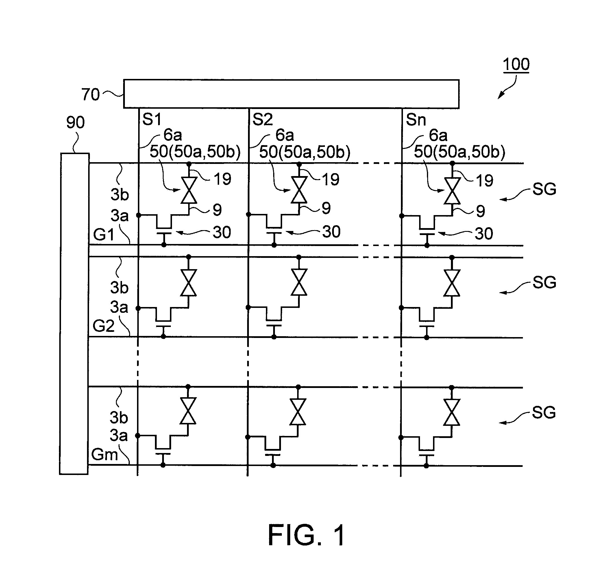
[0060]First will be described a liquid crystal device according to a first embodiment of the invention. FIG. 1 is an equivalent circuit diagram showing an electrical configuration of the liquid crystal device.

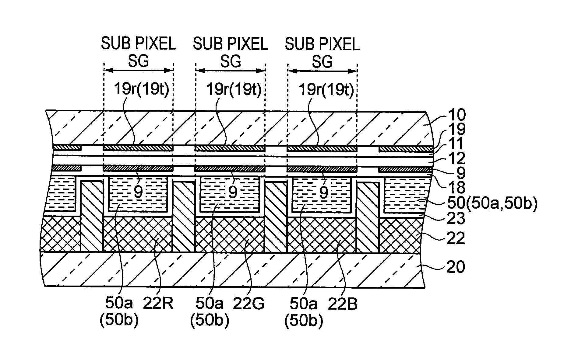
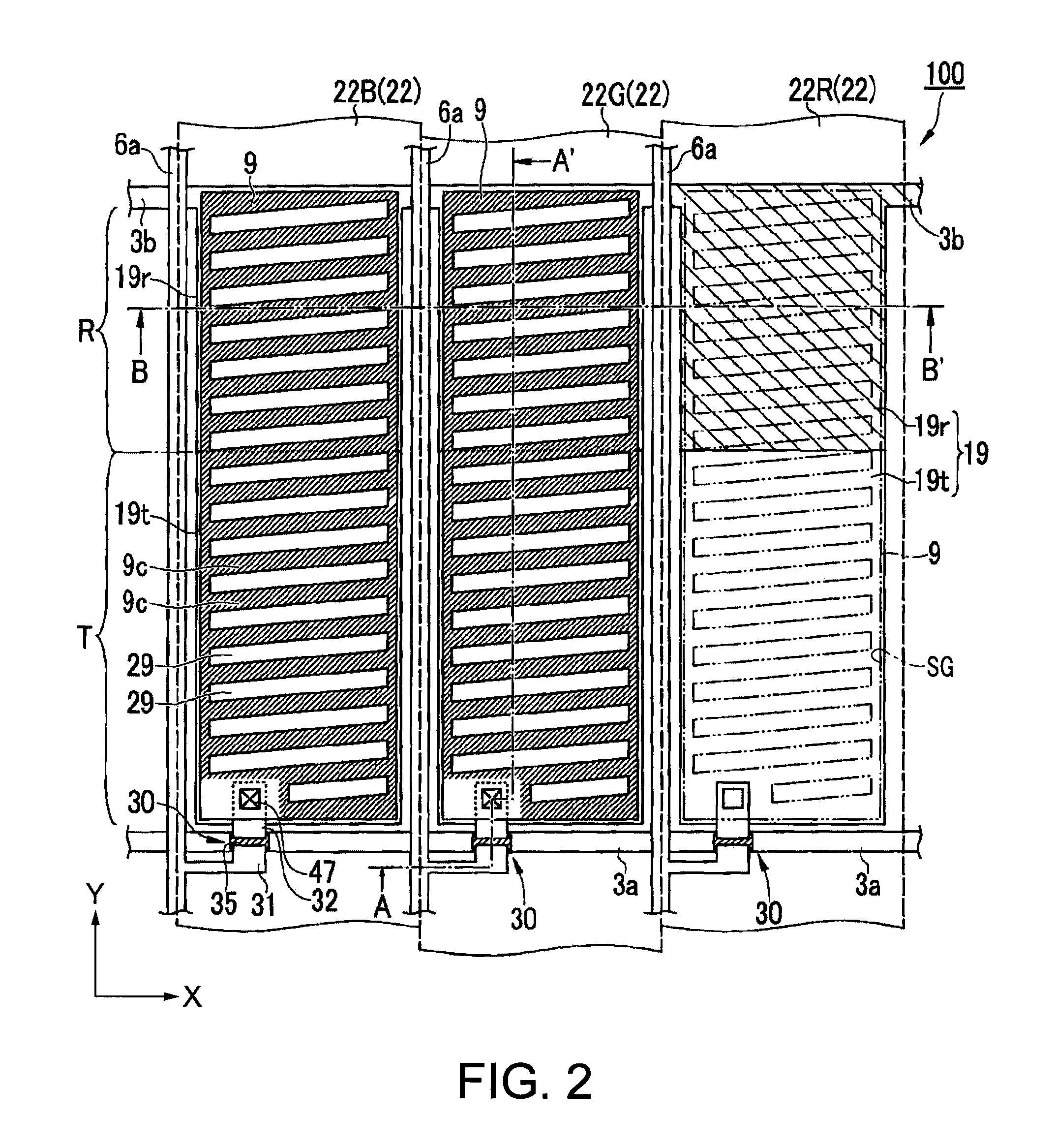
[0061]As shown in FIG. 1, a liquid crystal device 100 of the embodiment includes a plurality of sub pixels SG. Each of the sub pixels SG includes a pixel electrode 9, a common electrode 19, and a thin film transistor (TFT) 30 that switchingly controls the pixel electrode 9. Between the pixel electrode 9 and the common electrode 19 of the each sub pixel SG is interposed a liquid crystal layer 50. The liquid crystal layer 50 is composed of a first liquid crystal layer 50a and a second liquid crystal layer 50b, although details of the liquid crystal layer 50 will be described later. Each common electrode 19 is electrically connected to each of common lines 3b extended from a scan-line driving circuit 90 so as to be maintained at an electric potential com...

second embodiment

[0110]Another Liquid Crystal Device

[0111]Next will be described a liquid crystal device according to a second embodiment of the invention and a method for producing the liquid crystal device, with reference to drawings. FIGS. 8A and 8B schematically show sectional views of a structure of the liquid crystal device according to the second embodiment. The same constituent elements as those in the first embodiment are given the same reference numerals in the description below.

[0112]As shown in FIG. 8A, unlike the first embodiment, a liquid crystal device 800 of the second embodiment further includes a liquid-crystal-layer-thickness adjusting layer 25 (25G) that adjusts a thickness of the first liquid crystal layer 50a in the reflective display region R. Basic optical design conditions of the liquid crystal device 200 are the same as those of the liquid crystal device 100 of the first embodiment, and thus the conditions shown in FIG. 4 can be employed.

[0113]The liquid-crystal-layer-thick...

third embodiment

[0133]Electronic Apparatus

[0134]Next will be described a mobile phone as an example of an electronic apparatus according to a third embodiment of the invention. FIG. 11 is a schematic perspective view showing the mobile phone as the electronic apparatus.

[0135]As shown in FIG. 11, a mobile phone 300 of the third embodiment has a main body including an operating input section and a display section 301. The display section 301 incorporates the liquid crystal device 100 or 200 and an illumination device that illuminates the liquid crystal device. Accordingly, displayed information can be recognized by transmissive display using transmitted light from the illumination device and reflective display using incident light such as external light. That is, under a sufficiently bright condition such as an outdoor environment, reflective display enables information to be recognized without driving the illumination device. Thus, the mobile phone 300 realizes power consumption reduction and offers...


PUM


Abstract

A liquid crystal device includes a pair of substrates; a partition wall member that partitions a region sandwiched between the pair of substrates to provide reflective display regions and transmissive display regions; a plurality of pixels each including a plurality of pixel regions, each of the pixel regions having each of the reflective display regions and each of the transmissive display regions; and a first liquid crystal layer made of a first liquid crystal and a second crystal layer made of a second liquid crystal, the first and the second liquid crystal layers, respectively, being enclosed in the reflective display region and the transmissive display region, respectively, partitioned by the partition wall member so as to sandwich the first and the second liquid crystal layers between the pair of substrates, wherein a phase difference value of reflected light in the first liquid crystal layer is approximately equal to a phase difference value of transmitted light in the second liquid crystal layer.

Description

BACKGROUND[0001]1. Technical Field[0002]The present invention relates to a liquid crystal device including a reflective display region and a transmissive display region, a method for producing the liquid crystal device, and an electronic apparatus.[0003]2. Related Art[0004]Among liquid crystal devices, there is known a liquid crystal display including an array substrate having a plurality of scan lines and a plurality of signal lines mutually intersecting and an opposing substrate located on an opposite side of a liquid crystal layer from the array substrate. At intersections between the scan lines and the signal lines are provided respective pixels of red, blue, and green, each having a reflecting section having an external-light reflecting unit and a phase difference film. In the liquid crystal display, when phase difference values of the phase difference films in the respective red, blue, and green pixels are represented by rR, rG, and rB, respectively, at least one of expression...

Claims


Application Information

Patent Timeline
IPC IPC(8): G02F1/13363
CPCG02F1/133377G02F1/134363G02F1/133555G02F1/133512G02F1/1335G02F1/1343
Inventor SUZUKI, KATSUMIOTAKE, TOSHIHIRO
Owner SEIKO EPSON CORP
Why Eureka
Try Eureka