Systems and methods for link processing with ultrafast and nanosecond laser pulses

a laser pulse and ultrafast technology, applied in nuclear engineering, irradiation devices, manufacturing tools, etc., can solve the problems of increasing the risk of ic chips damage, deteriorating the quality of the device, and 1.3 m laser wavelengths with pulse widths in the nanosecond range. to reduce or eliminate the damage to the underlying passivation layer and/or substra

Inactive Publication Date: 2009-06-04
ELECTRO SCI IND INC
View PDF11 Cites 8 Cited by
  • Summary
  • Abstract
  • Description
  • Claims
  • Application Information

AI Technical Summary

Benefits of technology

[0009]The embodiments disclosed herein include systems and methods of using a combination of ultrafast and nanosecond laser pulses for processing elec

Problems solved by technology

However, the 1 μm and 1.3 μm laser wavelengths with pulse widths in the nanosecond range have disadvantages.
Such a conventional link processing laser pulse creates a large heat affected zone (HAZ) that could deteriorate the quality of the device that includes the severed link 22.
Increased laser pulse energy increases the damage risk t

Method used


Image

  • Systems and methods for link processing with ultrafast and nanosecond laser pulses
  • Systems and methods for link processing with ultrafast and nanosecond laser pulses
  • Systems and methods for link processing with ultrafast and nanosecond laser pulses

Examples


Embodiment Construction

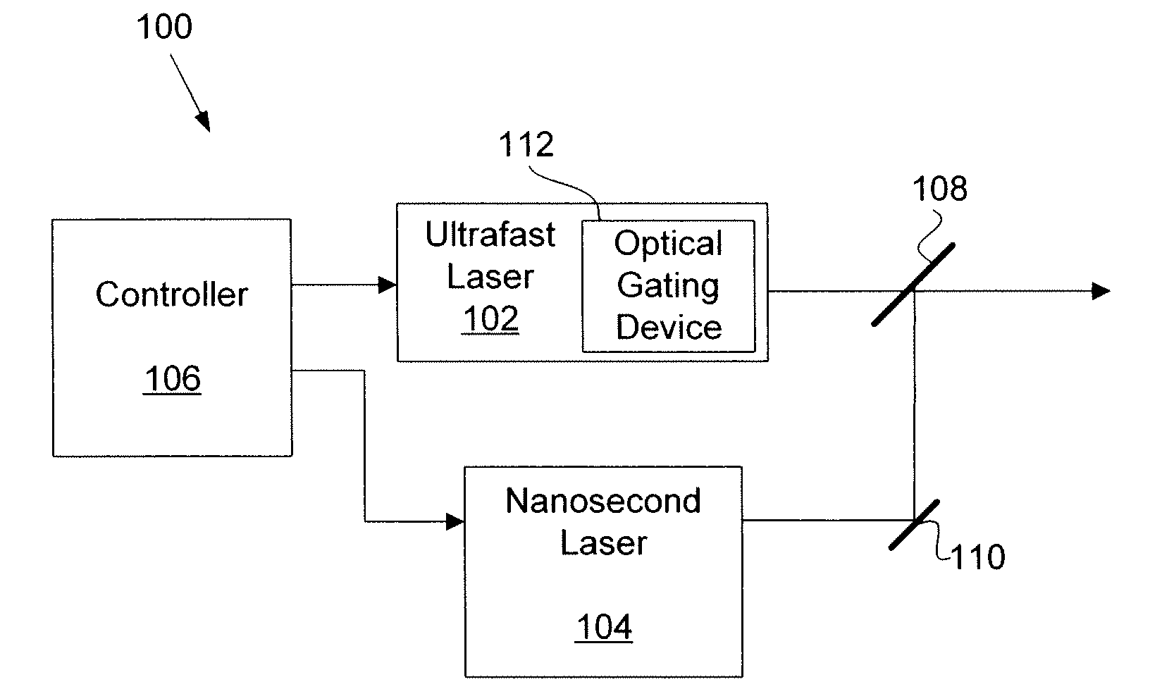
[0020]This disclosure describes the use of an ultrafast laser pulse, or a burst of ultrafast laser pulses, followed by one or more nanosecond laser pulses, with traditional temporal pulse shapes or specially tailored temporal pulse shapes, to process an electrically conductive link in an integrated circuit (IC).

[0021]The ultrafast laser pulse or pulses processes a passivation material overlying a link and a portion of the link material. In one such embodiment, the ultrafast laser pulse or pulses processes the overlying passivation layer based at least in part on laser intensity induced breakdown. In one embodiment, the ultrafast laser pulse or pulses processes a majority portion of the link.

[0022]Then, a nanosecond laser pulse completes the removal of the remaining link material. Because the processing provided by the nanosecond laser pulse is based mainly on heat generated through laser absorption by the target material and the underlying passivation material is a non-absorbing med...


PUM

PropertyMeasurementUnit
Timeaaaaaaaaaa
Timeaaaaaaaaaa
Timeaaaaaaaaaa

Abstract

Systems and methods for processing an electrically conductive link in an integrated circuit use a series of laser pulses having different pulse widths to remove different portions of a target structure without substantially damaging a material underlying the electrically conductive link. In one embodiment, an ultrafast laser pulse or bundle of ultrafast laser pulses removes an overlying passivation layer in a target area and a first portion of link material. Then, a nanosecond laser pulse removes a second portion of the link material to sever an electrical connection between two nodes in the integrated circuit. The nanosecond laser pulse is configured to reduce or eliminate damage to the underlying material.

Description

TECHNICAL FIELD[0001]This disclosure relates to laser processing of electrically conductive links in a memory or other integrated circuit (IC). In particular, this disclosure relates to laser systems and methods using both ultrafast and nanosecond laser pulses to sever electrically conductive links and to remove passivation material over the links.BACKGROUND INFORMATION[0002]Yields in IC device fabrication processes often incur defects resulting from alignment variations of subsurface layers or patterns of particulate contaminants. FIGS. 1, 2A and 2B show repetitive electronic circuits 10 of an IC device or work piece 12 that are commonly fabricated in rows or columns to include multiple iterations of redundant circuit elements 14, such as spare rows 16 and columns 18 of memory cells 20. The circuits 10 are also designed to include particular laser severable conductive links 22 between electrical contacts 24 that can be removed to disconnect a defective memory cell 20, for example, ...

Claims


Application Information

Patent Timeline
IPC IPC(8): G21K5/10H01S3/10H01S3/13
CPCH01L23/5258B23K26/0635B23K26/0624H01L2924/0002H01L2924/00
Inventor SUN, YUNLONGHARRIS, RICHARD S.
Owner ELECTRO SCI IND INC
Why Eureka
Try Eureka