Method of making an improved selective emitter for silicon solar cells

a selective emitter and solar cell technology, applied in semiconductor/solid-state device manufacturing, semiconductor devices, electrical equipment, etc., can solve the problems of high cost and undesirable effects of the art process used to achieve the selectively patterned emitter doping profile using lithographic or screen printing processing, and the difficulty of forming a low resistance contact to the layer

Inactive Publication Date: 2009-06-04
APPLIED MATERIALS INC
View PDF12 Cites 75 Cited by
  • Summary
  • Abstract
  • Description
  • Claims
  • Application Information

AI Technical Summary

Problems solved by technology

The dopant concentration in the phosphorous doped emitter is relatively low which improves junction characteristics but makes it difficult to form a low resistance contact to the layer.
However, the prior art processes utilized to accomplish this selectively patterned emitter doping profile using the lithographic or screen printing processing is costly and therefore undesirable.

Method used


Image

  • Method of making an improved selective emitter for silicon solar cells
  • Method of making an improved selective emitter for silicon solar cells
  • Method of making an improved selective emitter for silicon solar cells

Examples


Embodiment Construction

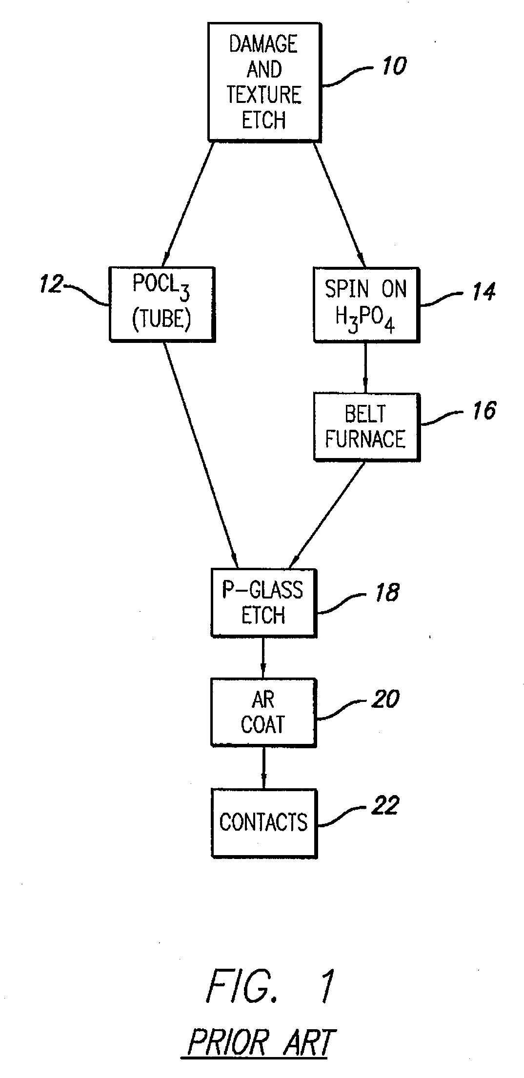
[0012]Referring now more particularly to FIG. 1, there is shown the traditional steps utilized in the processing of silicon solar cells. As is therein shown, the substrates which are formed of single-crystalline or multi-crystalline silicon wafers are etched as shown at 10 to eliminate damage which may be done at the time the wafer is formed. An etch done concurrently or immediately after the damage etch is also utilized to texture the surface of the substrate as is well known in the prior art. Subsequent to the damage plus the texture etch, the front surface of the substrate is processed to form an N-type layer in the P-type substrate. This is typically accomplished by applying a phosphorus compound such as a POCl3 layer on the front surface of the substrate and then diffusing the phosphorus from that layer into the surface of the substrate in a tube furnace as is shown at 12. Alternatively, the phosphorus may be applied to the front surface of the substrate by a spin-on process ut...


PUM


Abstract

A method for forming a selective emitter on a silicon solar cell is provided including forming an oxide layer on a surface of the P-type silicon substrate, implanting phosphorus doping atoms into the oxide layer on the substrate using plasma immersion ion implantation, patterning the oxide layer, annealing the substrate to provide heavily doped regions in the patterned regions and a lightly doped region between the patterned regions, and providing metal contacts to the heavily doped regions.

Description

FIELD OF THE INVENTION[0001]This invention pertains generally to silicon solar cells and improvements to their manufacture directed to improve the electrical and optical performance, more specifically, the invention pertains to the formation of a selective emitter utilizing improved processing techniques.BACKGROUND OF THE INVENTION[0002]Multi-crystalline silicon or single crystal silicon is used for the semiconductor substrate in the manufacture of silicon solar cells. Optimal solar cell performance depends on maximum absorption of light, minimized recombination, and minimized contact resistance at the junction between the crystalline semiconductor portion of the cell and the metal contacts used to collect charges and route current outside the cell.[0003]Typically such silicon solar cells are formed utilizing a P-type substrate material with an N-type region, typically one micron thick, formed on the front surface thereof with diffused phosphorous. This forms the emitter of the sola...

Claims


Application Information

Patent Timeline
Patent Type & Authority Applications(United States)
IPC IPC(8): H01L31/18H01L21/26
CPCH01L31/022425Y02E10/50H01L31/18
Inventor BORDEN, PETERTAYLOR, MITCHELL C.
Owner APPLIED MATERIALS INC
Why Eureka
Try Eureka