
Real time system for monitoring the commonality, sensitivity, and repeatability of test probes

Inactive Publication Date: 2009-06-04
IBM CORP
View PDF6 Cites 20 Cited by
  • Summary
  • Abstract
  • Description
  • Claims
  • Application Information

AI Technical Summary

Benefits of technology

[0022]It is yet a further object to provide statistical models that can be processed in the test system while testing takes place, allowing an automatic warning that can be set and triggered by the process code.
[0023]It is still a further object to substantially augment the probing effectiveness by including measurement sensitivity as well as commonality and repeatability to determine whether the tester meets the specified resolution at every test.
[0031]In still another aspect, the invention provides a real time evaluation on inherent tester specifications including the added accumulation of probe contact resistance inexistent in current probing methodology. The effectiveness of probing to measurement sensitivity and repeatability, in addition to the probe commonality can be quickly examined, helping the test engineer determine whether the tester meets the specified resolution at every test. It further allows the engineer to determine if the measured data range remains within an acceptable noise level which may be introduced by the measurement tool.

Problems solved by technology

The fabrication process of VLSI components includes a large number of manufacturing steps wherein effects are created leading to circuit malfunction and low performance.
Any variability of the test measurement tool, whether tester or probe card induced typically, reduces the repeatability and accuracy of the measurements being made.
A slight bending or soiled tip may be the cause of differences from other probes which may produce an impact on further device measurements that can no longer be detected from this test.b) A test technician aligning the probing tips on the designated probing pads on wafer at a predetermined site.
Depending on the training, experience and working attitude, generally this process does not ensure a reliable procedure to set up a test.
The above described methods fail to offer a reliable process that ensures the required high quality probing necessary for the next generation of testing wafers, and do not identify nor offer a finer resolution on the probe commonality.
By way of example, a soiled probing tip typically introduces a higher contact resistance which impacts the device measurement results and which if ignored, mislead the test engineer into making a wrong decision.
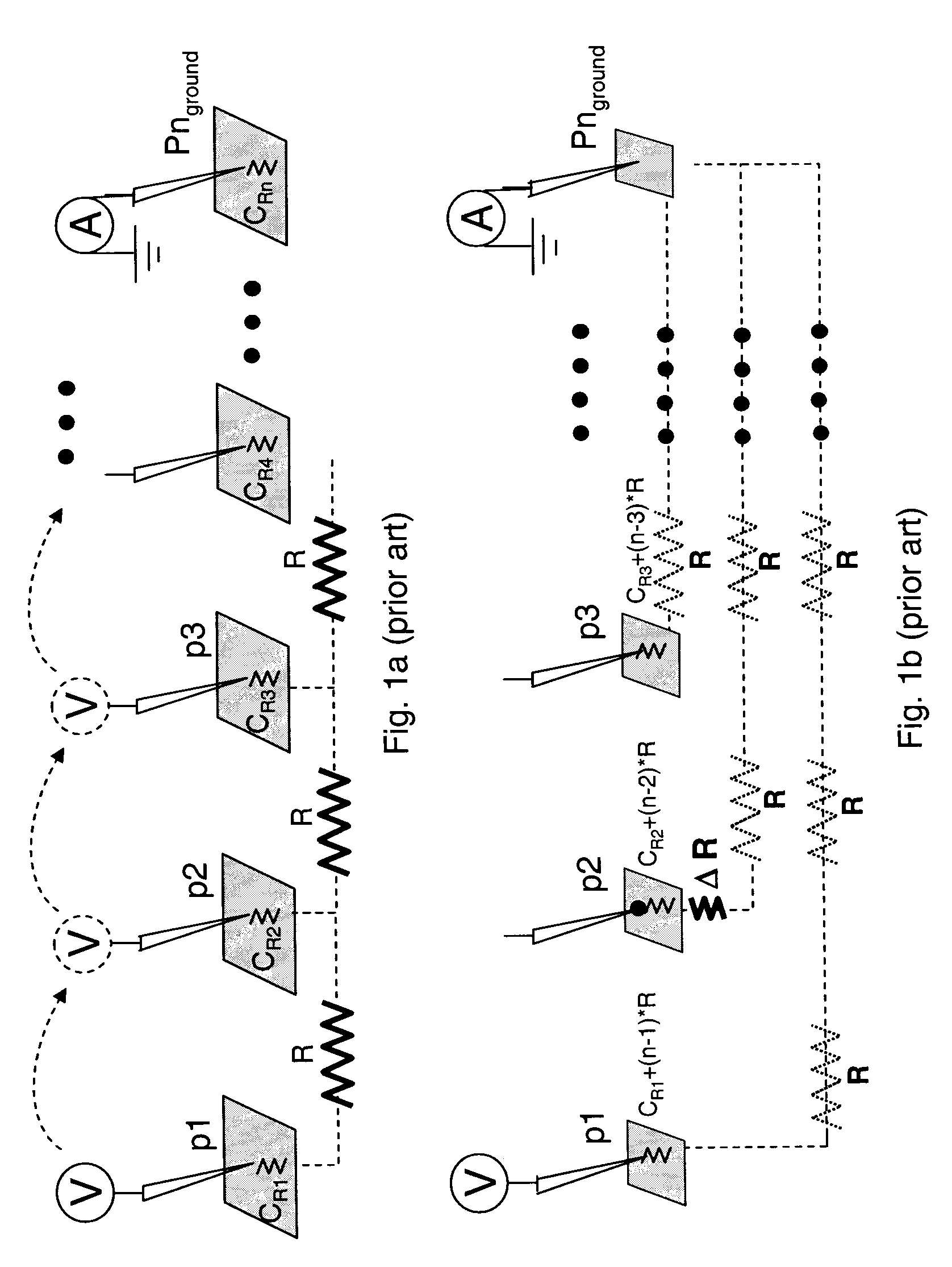
Due to inherent tester specifications (including drift resolution, repeatability, linearity) with the added accumulation of probe contact resistance (Cres), it is not realistic to assume that the tester / probe card combination becomes deterministic over time.
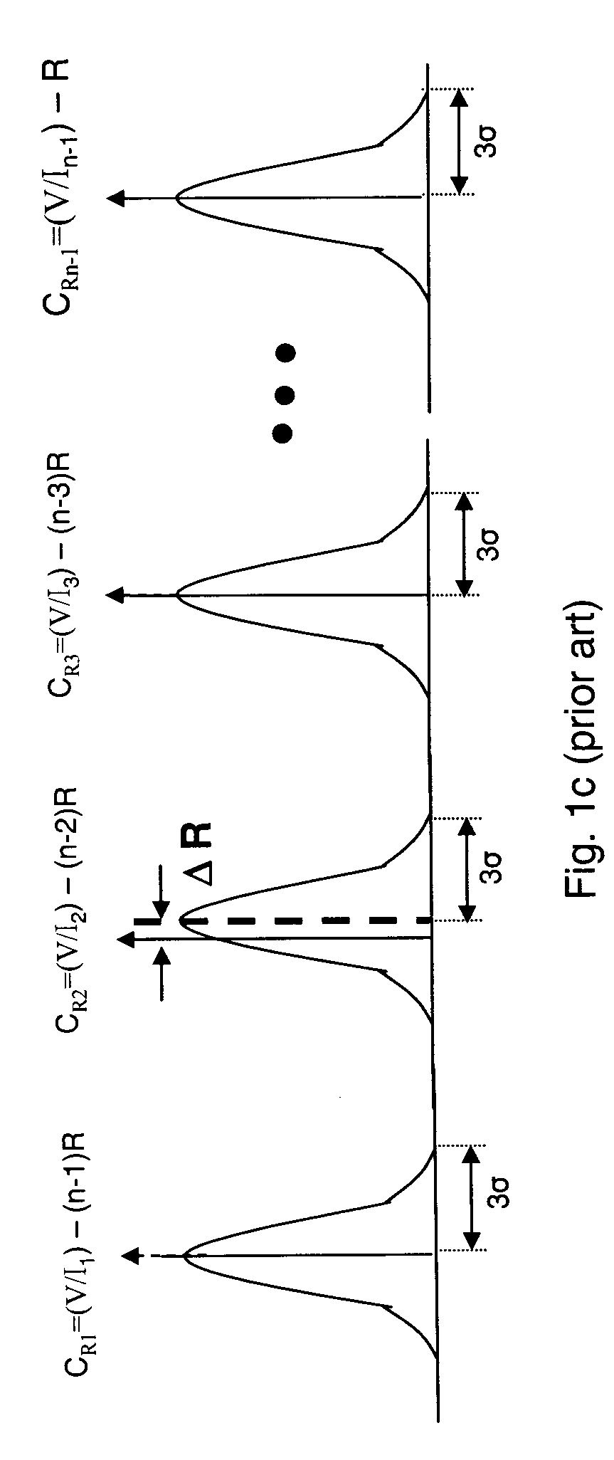
It is assumed that one probing tip, e.g., p2 does not make good contact to its corresponding landing pad, perhaps because the landing contact is not as clean as it should be.
The shift of ΔR may not cause a continuity test fail; yet, it may cause a significant impact on the transistor's performance characterization.
The test generates unreliable device data that may have a significant impact on the engineering time spent for device characterization, and on the quality of the end product.

Method used


Image

  • Real time system for monitoring the commonality, sensitivity, and repeatability of test probes
  • Real time system for monitoring the commonality, sensitivity, and repeatability of test probes
  • Real time system for monitoring the commonality, sensitivity, and repeatability of test probes

Examples


Embodiment Construction

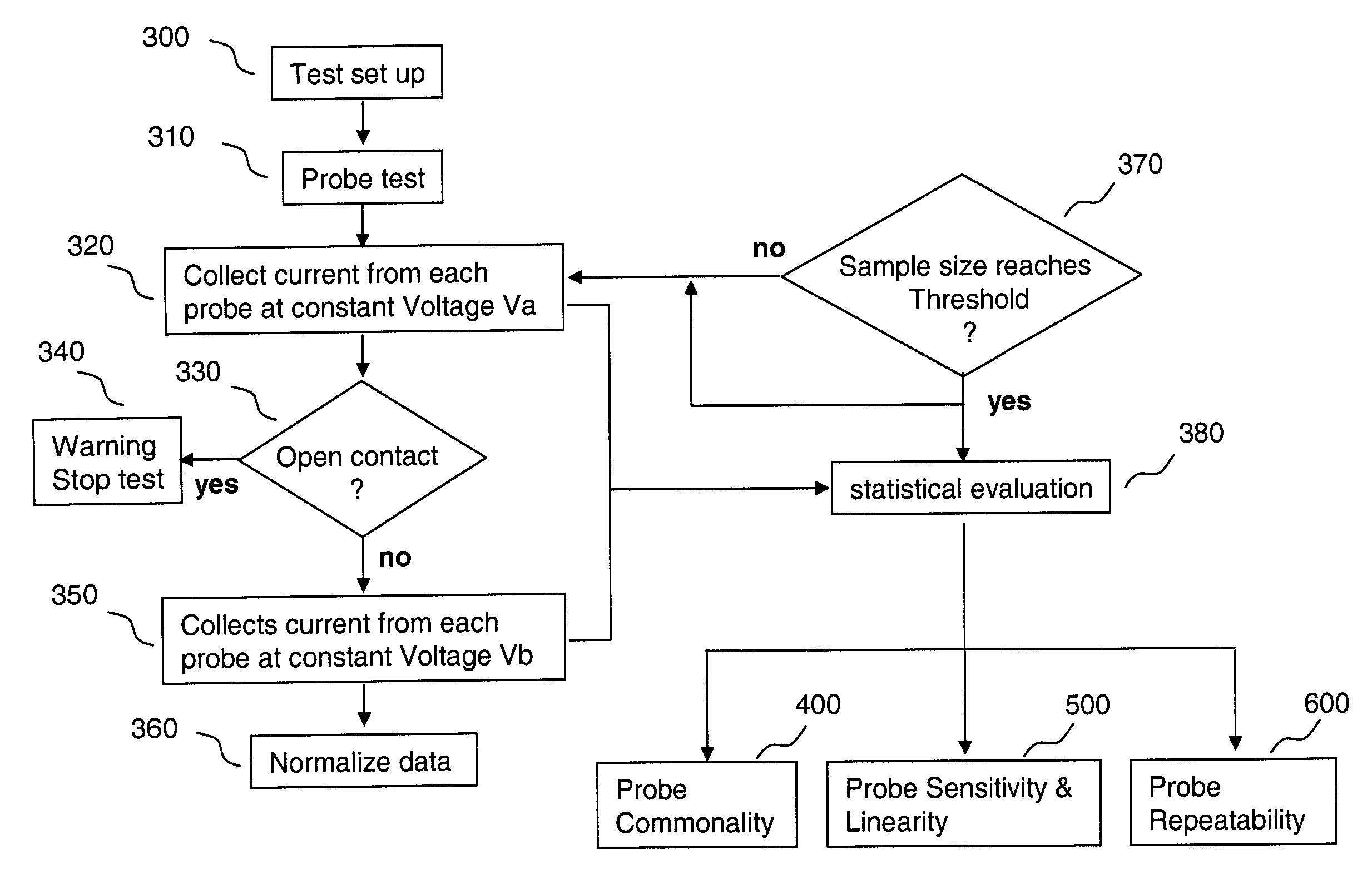
[0044]Referring to FIG. 2, there is shown a schematic diagram of the present invention for measuring the sensitivity and linearity of the test probes, wherein two sets of the normalized current distribution for each probe are obtained from applying two sets of voltage, Va and Vb, to each probe. The shifts of two populations of each probe resulting from the second applied voltage can be categorized in three categories, according to the present invention.

[0045]The first case shows probing pin, displaying a “low variability” and significant difference between two current populations, I1a and I2b, obtained by applying voltages Va and Vb, respectively. In addition, the linear behavior of Ohm's Law (V=I*R) applies to the shift of the mean of the two populations, i.e., mean_I1a / mean_I1b=Va / Vb.

[0046]The second case shows probing pin2 that indicates a “low variability” but an insignificant difference between the two populations, I2a and I2b, due to the delta of the mean value which is insuff...


PUM


Abstract

A system and a method for effectively determining the measurement sensitivity, repeatability, and probe commonality to assist a test engineer determine if the tester meets the specified resolution at every test. A statistical measurement of inherent tester specifications are provided with the added accumulation of the probe contact resistance during the probing process. It further provides a feedback to the test probe card noise level while testing is in progress. Moreover, the system and the method determine the test probing integrity in-situ when testing integrated circuit chips or wafers, dynamically detecting probing errors, and modifying data associated with defective test probes.

Description

FIELD OF THE INVENTION[0001]The present invention relates to the manufacture of semiconductor devices and packages, and more particularly, to a system and a method for monitoring the effectiveness of testing and probing wafers and IC chips.BACKGROUND OF THE INVENTION[0002]The fabrication process of VLSI components includes a large number of manufacturing steps wherein effects are created leading to circuit malfunction and low performance. By detecting manufacturing defects as well as characterizing the semiconductor devices performance, test equipment plays an important role that enables semiconductor manufacturers and designers to improve the manufacturing yield in addition to enhancing the quality and reliability of the end products.[0003]Numerous electrical test methods have been put in place to monitor the quality and integrity of the IC fabrication process. Probing a wafer is typically the first time that chips are tested to determine if they function as they are designed to do...

Claims


Application Information

Patent Timeline
IPC IPC(8): G01R31/26G06F19/00
CPCG01R31/2886G01R35/005G01R31/2894
Inventor KARTHIKEYAN, MUTHUKUMARASAMYMEDINA, LOUIS V.SONG, YUNSHENGTING, TSO-HUIWANG, PING-CHUAN
Owner IBM CORP
Learn More