Unlock instant, AI-driven research and patent intelligence for your innovation.

Semiconductor device including memory cell having charge accumulation layer

a memory cell and semiconductor technology, applied in the direction of pulse automatic control, pulse technique, instruments, etc., can solve the problem of enlarge the circuit area

Active Publication Date: 2009-06-11
KIOXIA CORP
View PDF5 Cites 34 Cited by
  • Summary
  • Abstract
  • Description
  • Claims
  • Application Information

AI Technical Summary

Benefits of technology

The present invention relates to a semiconductor device with MOS transistors and capacitor elements. The device includes a voltage generating circuit that generates voltage from the current paths of the MOS transistors and applies it to a memory cell for holding data. The device also includes a contact plug that connects the MOS transistors or one of them and a capacitor element. The distance between the gate and the contact plug is larger for the first MOS transistor than for the second MOS transistor. The technical effect of this invention is to provide a semiconductor device with improved voltage generation and data storage capabilities.

Problems solved by technology

Therefore, in order to secure a sufficiently-boosted voltage, unfortunately, the number of stages of the rectifying element is increased, which enlarges the circuit area.

Method used


Image

  • Semiconductor device including memory cell having charge accumulation layer
  • Semiconductor device including memory cell having charge accumulation layer
  • Semiconductor device including memory cell having charge accumulation layer

Examples


first embodiment

[0048]A semiconductor device according to a first embodiment of the invention will be described below. FIG. 1 is a block diagram showing a configuration of a part of a NAND type flash memory according to the first embodiment.

[0049]

[0050]Referring to FIG. 1, the NAND type flash memory 1 includes a memory cell array 2, a row decoder 3, a voltage generating circuit 4, and a control circuit 5.

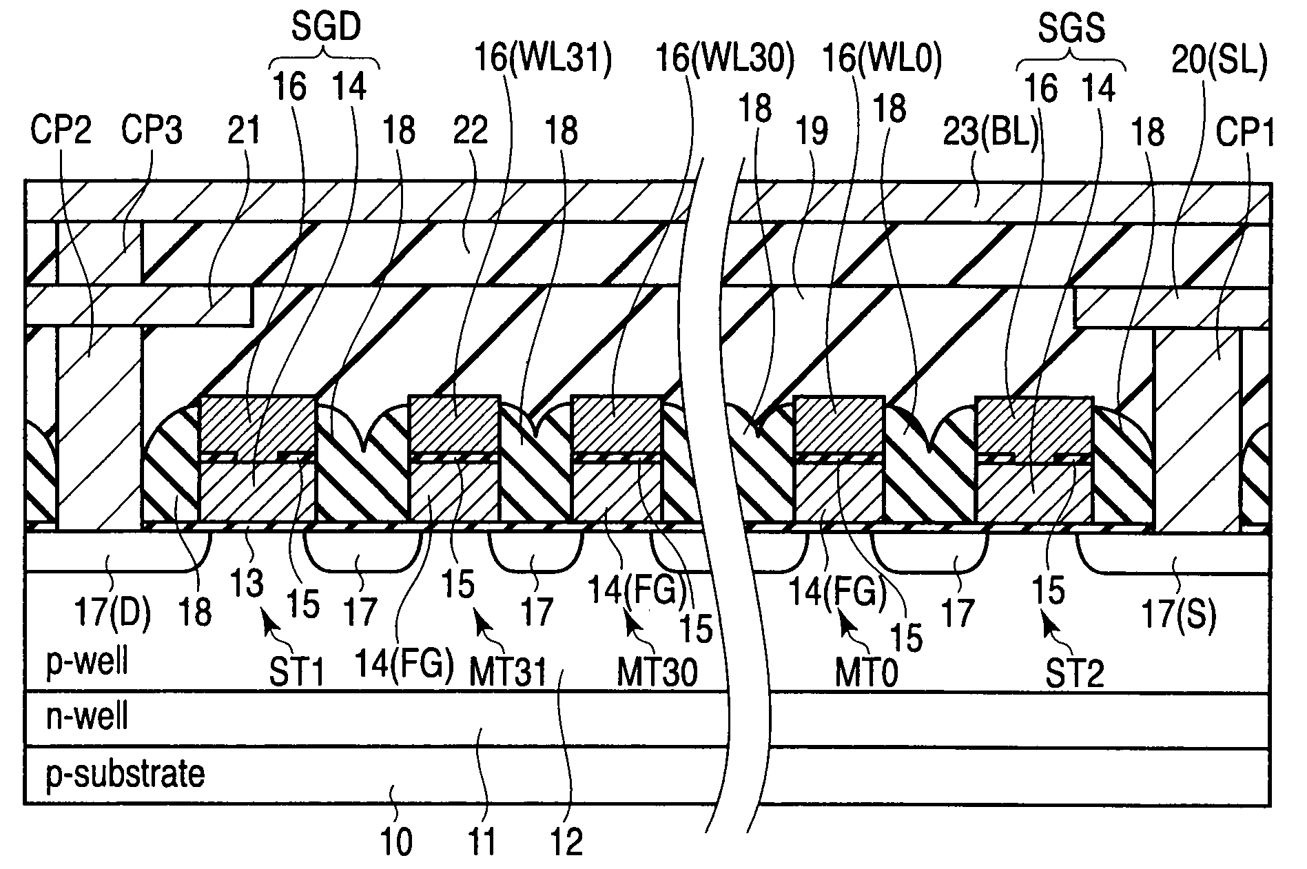
[0051]The memory cell array 2 includes plural memory cell transistors MT, and the data can be retained in each of the memory cell transistors MT. Each of the memory cell transistors MT includes a stacked gate in which a charge accumulation layer and a control gate are stacked. The charge accumulation layer can retain charges. The control gate is formed on the charge accumulation layer. In each memory cell transistor MT, the control gate is connected to a word line WL, a drain is electrically connected to a bit line BL, and a source is electrically connected to a source line SL.

[0052]The row decoder...

second embodiment

[0210]A semiconductor device according to a second embodiment of the invention will be described. In the second embodiment, a three-phase clock is used in the configuration according to the first embodiment. Only the points different from the first embodiment will be described below.

[0211]FIG. 33 is a circuit diagram showing a charge pump circuit 6 of the second embodiment. In FIG. 33, respective broken lines indicate that the MOS transistors TR located therein have the same dimensions, respectively. As shown in FIG. 33, the charge pump circuit 6 of the second embodiment differs from the charge pump circuit 6 according to the first embodiment in the following points. A clock φ3-1 is input into the other electrode of the capacitor element Cj connected to the node Nj (j=1, 4, and 7). A clock φ3-2 is input into the other electrode of the capacitor element C(j+1) connected to the node N(j+1). A clock φ3-3 is input into the other electrode of the capacitor element C(j+2) connected to the...

third embodiment

[0213]A semiconductor device according to a third embodiment of the invention will be described. In the third embodiment, a four-phase clock is used in the configuration according to the first embodiment. Only the points different from the first embodiment will be described below.

[0214]FIG. 35 is a circuit diagram showing a charge pump circuit 6 of the third embodiment. In FIG. 35, respective broken lines indicate that the MOS transistors TR located therein have the same dimensions, respectively. As shown in FIG. 35, the charge pump circuit 6 of the third embodiment differs from the charge pump circuit 6 according to the first embodiment in the following points. A clock φ4-1 is input into the other electrode of the capacitor element Cj connected to the node Nj (j=1 and 5). A clock φ4-2 is input into the other electrode of the capacitor element C(j+1) connected to the node N(j+1). A clock φ4-3 is input into the other electrode of the capacitor element C(j+2) connected to the node N(j...


PUM


Abstract

A semiconductor device includes MOS transistors, capacitor elements, a voltage generating circuit, a contact plug, and a memory cell. The MOS transistor and the capacitor element are formed on a first one of the element regions and a second one of the element regions, respectively. In the voltage generating circuit, current paths of the MOS transistors are series-connected and the capacitor elements are connected to the source or drain of the MOS transistors. The contact plug is formed on the source or the drain to connect the MOS transistors or one of the MOS transistors and one of the capacitor elements. A distance between the gate and the contact plug both for a first one of the MOS transistors located in the final stage in the series connection is larger than that for a second one of the MOS transistors located in the initial stage in the series connection.

Description

CROSS-REFERENCE TO RELATED APPLICATIONS[0001]This application is based upon and claims the benefit of priority from prior Japanese Patent Application No. 2007-317582, filed Dec. 7, 2007, the entire contents of which are incorporated herein by reference.BACKGROUND OF THE INVENTION[0002]1. Field of the Invention[0003]The present invention relates to a semiconductor device including a memory cell having a charge accumulation layer. For example, the invention relates to a configuration of a semiconductor device provided with a NAND type flash memory.[0004]2. Description of the Related Art[0005]Conventionally, an EEPROM (Electrically Erasable and Programmable Read Only Memory) is known as a nonvolatile semiconductor memory. Usually, the memory cell of an EEPROM has a MISFET structure including a stacked gate in which a charge accumulation layer and a control gate are stacked on a semiconductor substrate. Data is stored in the memory cell in a nonvolatile manner by a difference in thresho...

Claims


Application Information

Patent Timeline
Patent Type & Authority Applications(United States)
IPC IPC(8): H03L7/00H01L29/94H01L29/792H10B12/00H01L21/336H01L21/822H01L21/8234H01L27/04H01L27/06H01L27/088H01L27/10H01L29/788H02M3/07H03K17/06H03K19/00H10B41/40H10B43/40H10B69/00
CPCH01L27/0207H01L27/0222H01L27/105H01L27/115G11C16/30H01L27/11526H01L27/11529G11C16/24H01L27/11519H10B41/10H10B41/40H10B41/41H10B69/00H01L21/76897
Inventor NOGUCHI, MITSUHIROGOMIKAWA, KENJI
Owner KIOXIA CORP