Method for correcting mask pattern, and exposure mask

Inactive Publication Date: 2009-06-11
ELPIDA MEMORY INC
View PDF6 Cites 15 Cited by
  • Summary
  • Abstract
  • Description
  • Claims
  • Application Information

AI Technical Summary

Benefits of technology

[0020]The first aspect of the present invention provides a method for correcting optical proximity effect of a mask pattern for exposure light, the mask pattern including a rectangular pattern formed by a transparent region having a dimension of limiting resolution of exposure light, comprising: performing exposure by means of an evaluating mask on which an evaluation pattern including the rectangular pattern is arranged so as to form a pattern on a wafer; calculating an error between a simulation value obtained by a simulation of exposure, the simulation using the evaluation pattern and a dimension value of the pattern formed on the wafer; and optimizing a simulation parameter so that the error becomes small, wherein the simulation parameter comprises at least a first bias value and a second value, the first bias value corrects a corner portion of the rectangular pattern, and the second bias value corrects a side portion of the rectangular pattern.
[0021]The second aspect of the present invention provides an exposure mask manufactured based on mask data, wherein the mask data undergoes correction of the optical proximity effect by a method for correcting optical proximity effect of a mask pattern for exposure light, the mask pattern including a rectangular pattern formed by a transparen

Problems solved by technology

However, it is known that the resolution enhancement technique that is effective in the dense pattern has adverse effects such as a reduction in the depth of focus when a sparse pattern in which the diffracted light is not generated partly exists.
Although the application of the resolution enhancement technique enhances resolution, a considerable amount of information of the mask pattern that is formed on a mask is lost on a wafer that is an imaging surface, which results in a problem in which the deformation and dimensional fluctuations of a resist pattern are generated on the wafer.
Thus, the dimensional difference in the pattern on the wafer becomes large, thereby causing apparent deformation in a two-dimensional pattern.
However, the rule based OPC has a problem in which vast amounts of man hours are required to create the rule.
However, the OPC process itself of the model based OPC is known to be slower than that of the rule based

Method used


Image

  • Method for correcting mask pattern, and exposure mask
  • Method for correcting mask pattern, and exposure mask
  • Method for correcting mask pattern, and exposure mask

Examples


first exemplary embodiment

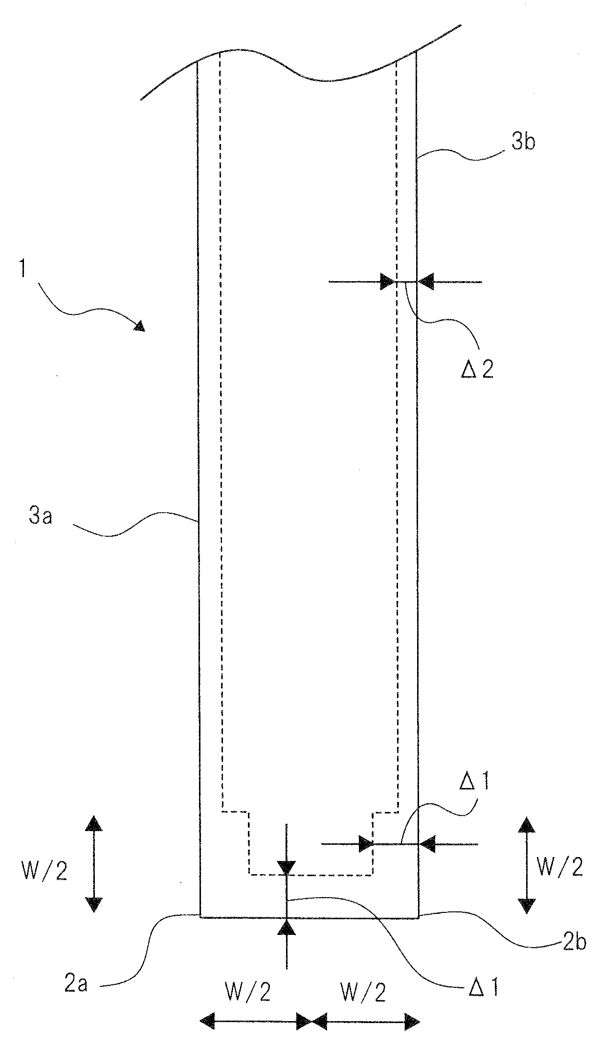
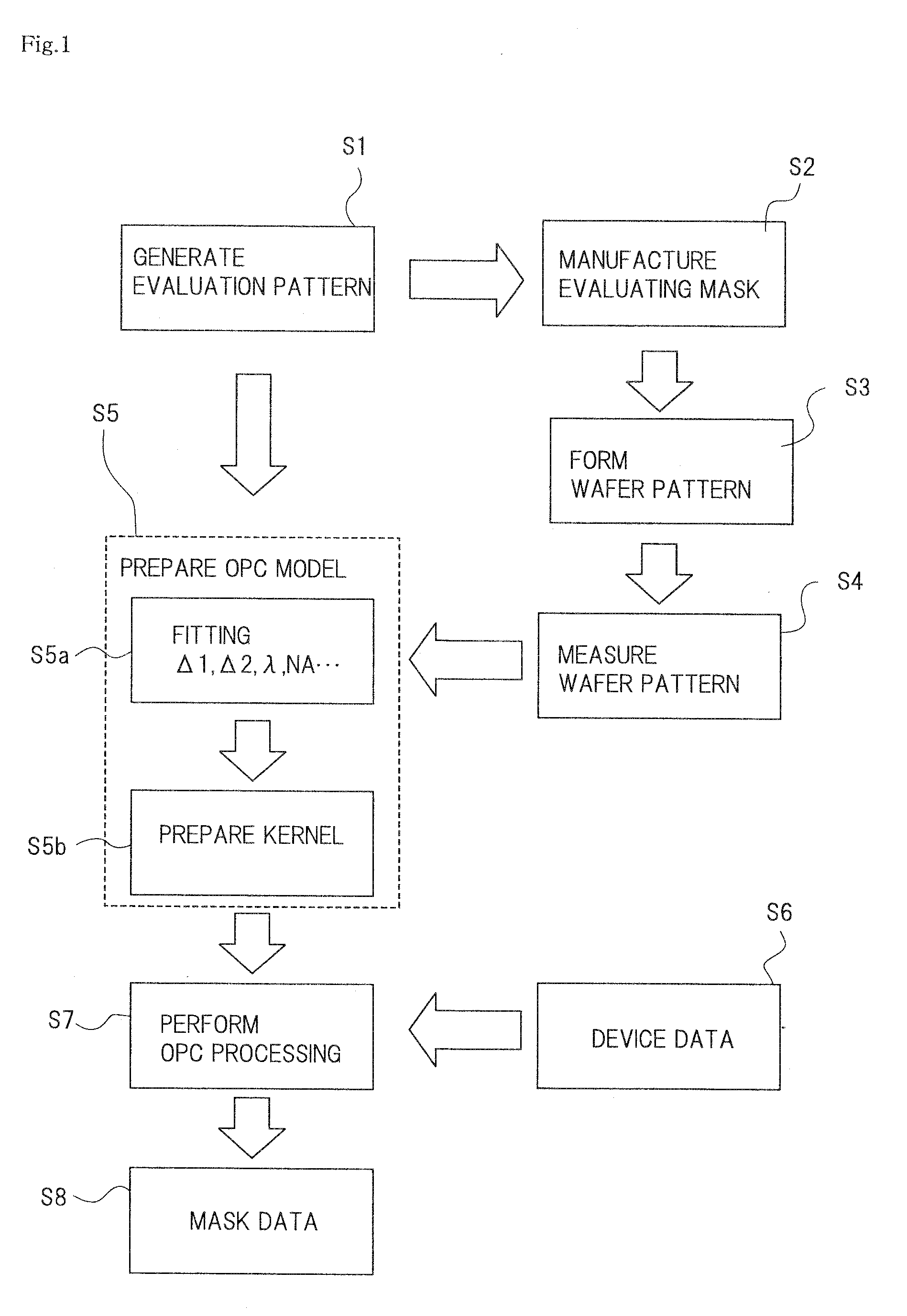
[0030]FIG. 1 is a flowchart illustrating a method for correcting a mask pattern according to a first exemplary embodiment of the present invention, where there is shown a procedure for obtaining mask data in order to prepare an exposure mask, hereinafter simply called a “mask”. The mask is used in an exposure process, by which a desired device pattern, where a hole pattern and a space pattern are mixed on a wafer (not shown), is formed. An ArF exposure device (exposure wavelength λ=193 nm) which uses the mask has a reduction magnification of 4, and the optical condition is ordinary lighting of NA=0.92 and coherent factor σ=0.5.

[0031]The mask is a halftone phase shifting mask. This mask is formed by a transparent substrate using synthetic quartz (SiO2), and a translucent film (film thickness=71.85 nm, permeability=5%) using molybdenum silicide oxide and nitride (MoSiON) and the like. The refractive index (n, k) of the transparent substrate is (1.474, 0) at the exposure wavelength of ...

second exemplary embodiment

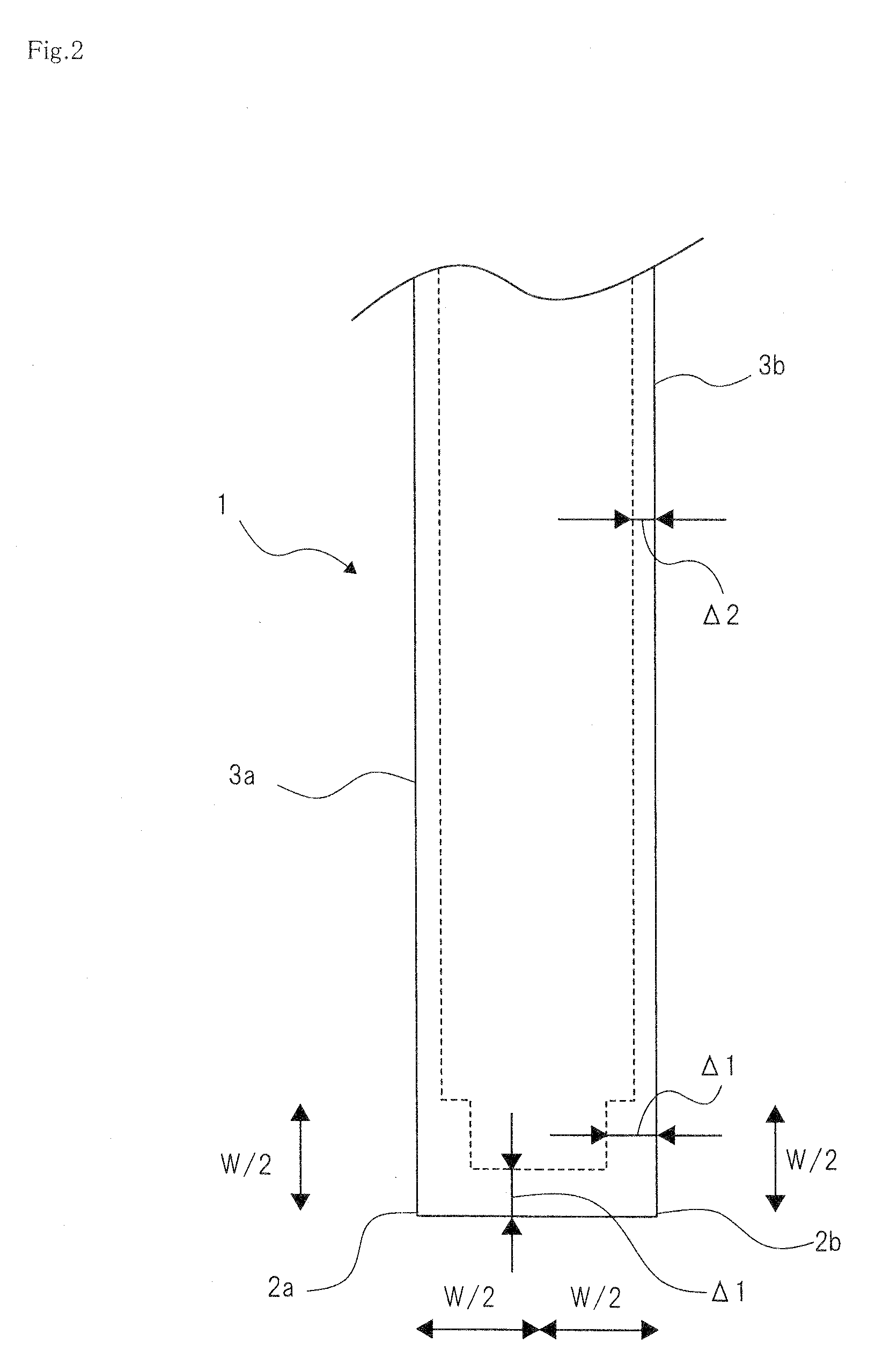
[0046]FIG. 3 is a flowchart illustrating a method for correcting a mask pattern according to a second exemplary embodiment of the present invention. For portions of descriptions that overlap with those of the method for correcting a mask pattern illustrated in FIG. 1, those descriptions will not be repeated below as needed. The method for correcting a mask pattern according to this exemplary embodiment is mainly different from that illustrated in FIG. 1, wherein a rule based OPC as well as a model based OPC is applied. For example, as a rule for correcting a side, a bias value Δ2 is calculated by means of simulation (refer to FIG. 4). Then, as a rule for correcting a corner, a bias value Δ1 is calculated by an experiment (refer to FIG. 5). Then, using these bias values Δ1, Δ2, the rule based OPC is performed.

[0047]First, in the method for correcting a mask pattern, a bias value Δ2 of a side of a rule used for the rule based OPC is previously calculated by means of simulation. FIG. 4...


PUM


Abstract

A method for correcting optical proximity effect of a mask pattern for exposure light, the mask pattern including a rectangular pattern formed by a transparent region having a dimension of limiting resolution of exposure light, includes (a) performing exposure by means of an evaluating mask on which an evaluation pattern including the rectangular pattern is arranged so as to form a pattern on a wafer. Further, the method includes (b) calculating an error between a simulation value obtained by a simulation of exposure, the simulation using the evaluation pattern and a dimension value of the pattern formed on the wafer, and (c) optimizing a simulation parameter so that the error becomes small. The simulation parameter includes at least a first bias value and a second value, the first bias value corrects a corner portion of the rectangular pattern, and the second bias value corrects a side portion of the rectangular pattern.

Description

BACKGROUND OF THE INVENTION[0001]1. Field of the Invention[0002]The present invention relates to a method for correcting a mask pattern, and an exposure mask. This invention particularly relates to a method for correcting a mask pattern used to form a desired device pattern on a wafer, and an exposure mask manufactured by the method.[0003]2. Description of Related Art[0004]In the present optical lithography technology, a shortened wavelength (λ) of exposure light used in an exposure device, a high numerical aperture (NA) of a projector lens and a resolution enhancement technique are applied, whereby a fine pattern 1 / 2 times or less as large as the exposure wavelength can be formed. Generally, resolution R is expressed by R=k1·λ / NA. This NA is defined by NA=n·sin θ, where θ is a maximum incidence angle at an imaging surface and indicates the magnitude of a projector lens, that is, this magnitude represents how much light that is diffracted by a mask is collected. This n is a refracti...

Claims


Application Information

Patent Timeline
IPC IPC(8): G03F1/00G03F1/32G03F1/36G03F1/68H01L21/027
CPCG03F1/36G03F1/144G03F1/68
Inventor YASUZATO, TADAO
Owner ELPIDA MEMORY INC
Why Eureka
Try Eureka