Method for manufacturing semiconductor device and substrate processing apparatus

a technology of substrate processing and semiconductor devices, which is applied in the direction of liquid surface applicators, coatings, chemical vapor deposition coatings, etc., can solve the problems of metallic contamination, reduced film formation speed (film formation rate) sometimes, and foreign substances in the processing chamber. achieve the effect of adequate etching ra

Inactive Publication Date: 2009-06-11
KOKUSA ELECTRIC CO LTD
View PDF12 Cites 30 Cited by
  • Summary
  • Abstract
  • Description
  • Claims
  • Application Information

AI Technical Summary

Benefits of technology

[0098]FIG. 6 shows the results of verification on the temperature dependency of the etching rate and the selection ratio in the cleaning method according to the present embodiment.
[0099]FIG. 6A is a graph showing temperature dependency of an etching rate of silicon nitride film, an etching rate of quartz, and a selection ratio (the etching rate of silicon nitride film / the etching rate of quartz), respectively. FIG. 6B is a table showing the data on which the graph is based. In FIG. 6A, the left vertical axis shows the etching rates of silicon nitride film and quartz (Å / min), and the right vertical axis shows the selection ratio (the etching rate of silicon nitride film / the etching rate of quartz). The horizontal axis shows the temperature in the processing chamber 201. In the graphs, black dots show the etching rates of silicon nitride film, and white dots show the etching rates of quartz, and the “+” marks show the selection ratios. A silicon nitride film subject to etching was formed under the processing conditions in the range exemplified in the above-described embodiment. Etching was performed by changing the temperature to 300° C., 350° C., 400° C., 450° C., and 500° C. Other etching conditions than temperature were set to: pressure: 100 Torr, F2 flow rate: 2 slm, the N2 flow rate: 8 slm, and F2 concentration (F5 / (F2+N2)): 20%.
[0100]It is found from FIG. 6 that both the etching rate of silicon nitride film and the etching rate of quartz increase as the temperature increases, and that, on the contrary, the selection ratio decreases as the temperature increases.
[0101]It is also found that, etching of silicon nitride hardly progresses at a temperature of approx. 300° C., and that it sufficiently advances at a temperature not less than 350° C. enabling a silicon nitride film to be etched at an adequate etching rate.
[0102]It is found from that, etching of quartz does not progress much at a temperature less than 400° C., such as 300° C., 350° C., or the like, and that it sufficiently advances at a temperature not less than 400° C. and not more than 450° C., enabling quartz to be etched at an adequate etching rate, although the etching rate of quartz is lower than the etching rate of silicon nitride film.
[0103]In addition, at 450° C., the selection ratio is approx. 1 (1.2) and the etching rate of silicon nitride film is substantially equal to the etching rate of quartz. Based on this, it is found that silicon nitride film and quartz are etched equally.

Problems solved by technology

When the thickness of the deposited material reaches or exceeds a certain thickness, the deposited material peels from the inner wall, or the like, of the processing chamber, which may cause generation of foreign substances (particles) in the processing chamber.
However, when the above-described dry cleaning is performed, the film formation speed (film formation rate) is sometimes decreased in the thin film formation process which is immediately after the dry cleaning.
However, in this method, the HF gas which has been added, or HF gas generated by the reaction of F2 gas and H2 gas sometimes causes metallic contamination due to corrosion of a metal member in the processing chamber or breakage of a quartz member in the processing chamber due to erosion.

Method used


Image

  • Method for manufacturing semiconductor device and substrate processing apparatus
  • Method for manufacturing semiconductor device and substrate processing apparatus
  • Method for manufacturing semiconductor device and substrate processing apparatus

Examples


example 1

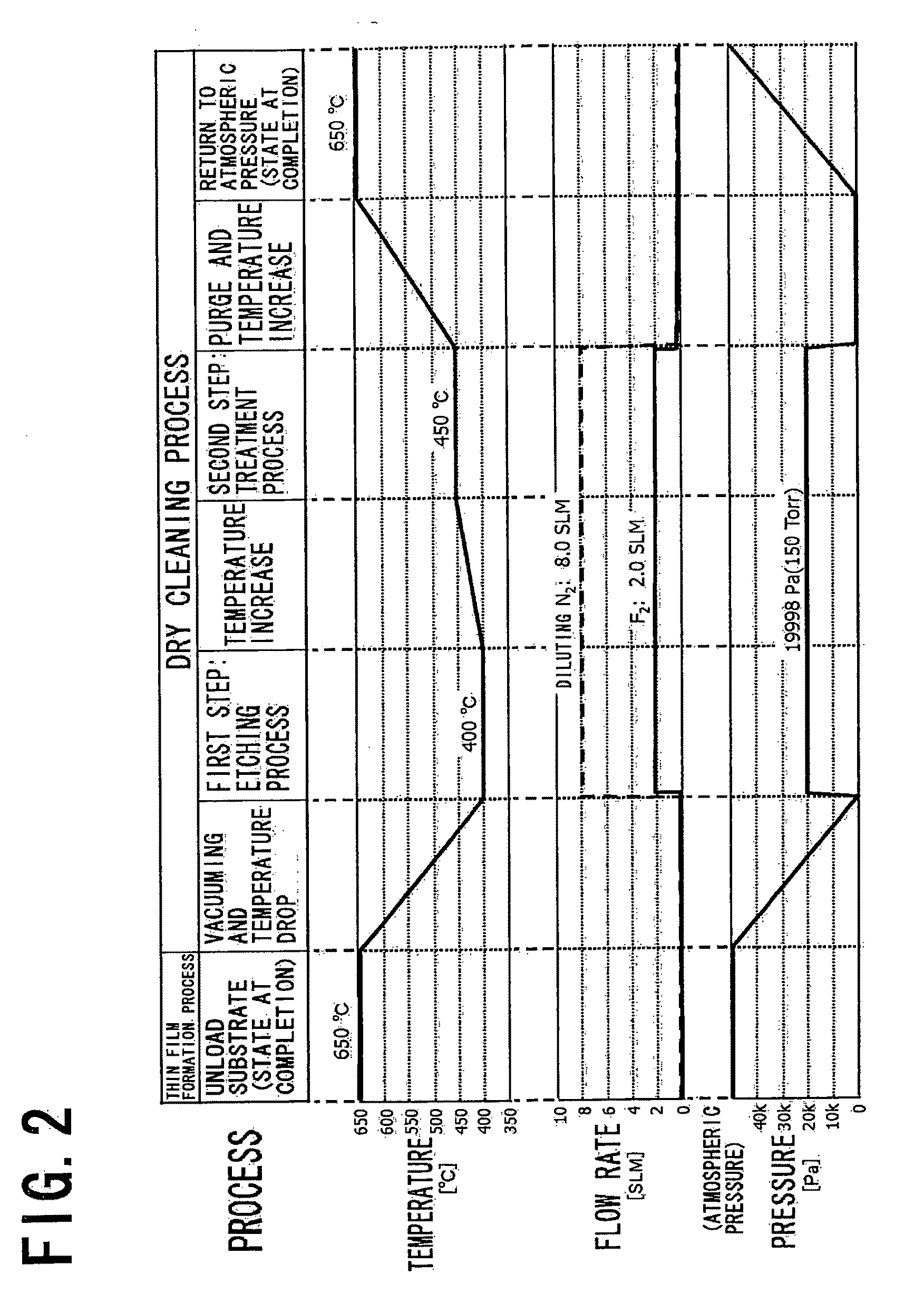
[0119]As Example 1 of the present invention, a case where the cleaning is performed, with the temperature (second temperature) in the processing chamber 201 in the second step (treatment process) being set higher than the temperature (first temperature) in the processing chamber 201 in the first step (thin film etching process) will be described. FIG. 2 is a graph chart showing the sequence and the cleaning conditions of the cleaning step according to the Example 1 of the present invention.

[0120]In the thin film formation process of Example 1, a silicon nitride film was formed with use of SiH2Cl2 (DCS) gas and NH3 gas, as the processing gas, in accordance with the same method and conditions as those in the above-described embodiment. The film thickness of the silicon nitride to be formed by a single thin film formation process was set to 500 Å. After the thin film formation process was performed 16 times (every time when cumulative film thickness becomes 8000 Å), the cleaning proces...

example 2

[0123]As Example 2 of the present invention, a case where the cleaning step was performed, with both the temperature (first temperature) in the processing chamber 201 in the first step (thin film etching process) and the temperature (second temperature) in the processing chamber 201 in the second step (treatment process) being set to 450° C., will be described. FIG. 3 is a graph chart showing the sequence and the cleaning conditions of the cleaning according to the Example 2 of the present invention. Other conditions are the same as those in the Example 1.

[0124]As is the case with the Example 1, the 16 times of the thin film formation processes and the subsequent cleaning step were assumed as 1 cycle. Next, the cycle was repeated a plurality of times. Every time the thin film formation process is completed, the amount of increased foreign substances in the processing chamber 201 was measured, and the film formation rate of silicon nitride film was also measured.

[0125]In both the Exa...

example 3

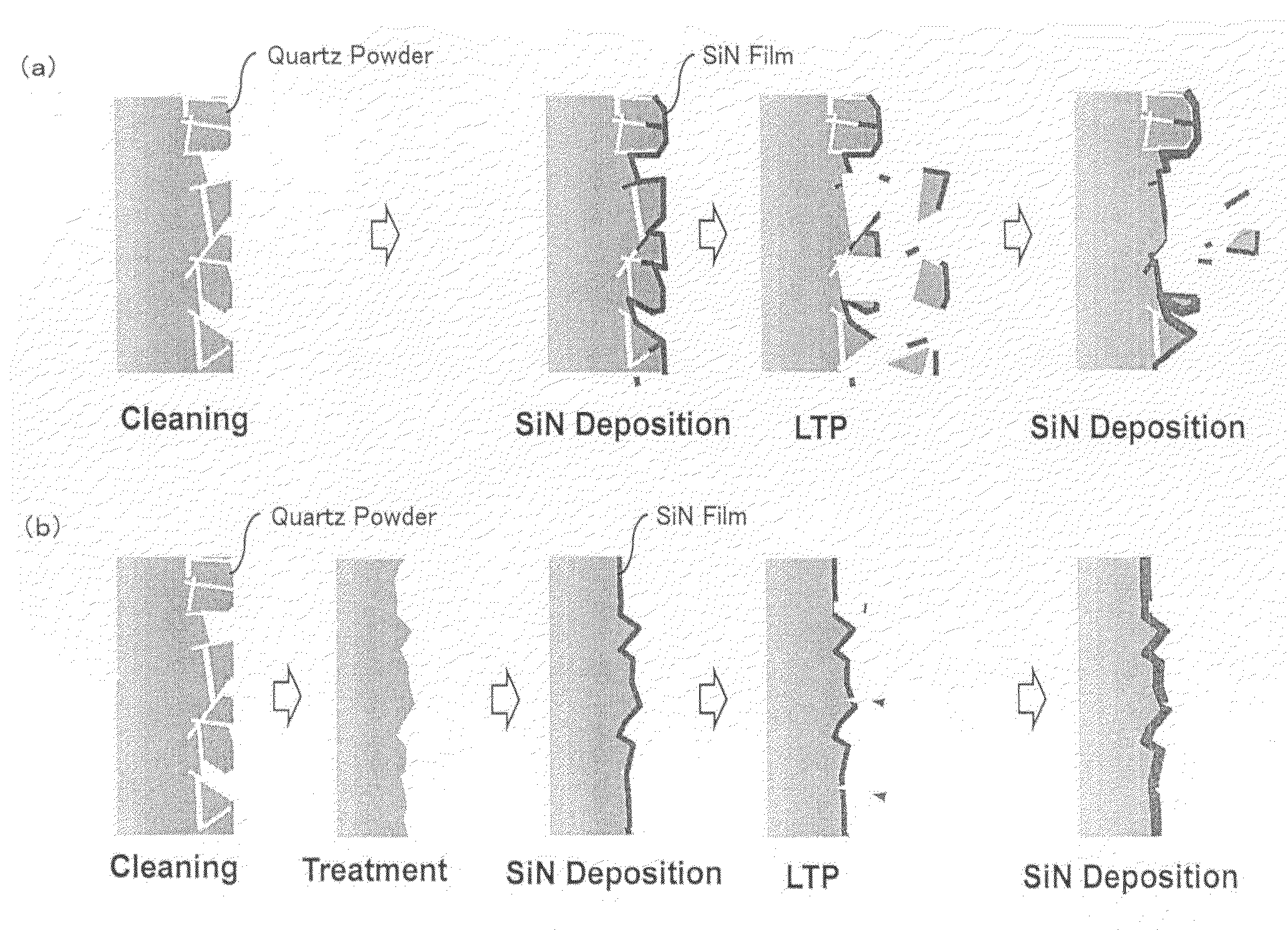
[0130]As Example 3 of the present invention, a case in which the cleaning in the above-described embodiment (Example 1, Example 2) and LTP (Low Temperature Purge) are combined will be described. The LTP, also called as the low temperature purge, herein refers to purge of the inside of the processing chamber 201 with gas, while applying a thermal impact onto the thin film deposited on the inside of the processing chamber 201 by decreasing a temperature in the processing chamber 201, so as to forcibly generate a crack in the thin film and forcibly peel the adhered material adhered on the inside of the processing chamber with a weak adhesive force.

[0131]In the meantime, the above-described embodiment (Example 1, Example 2) is an art based on the assumption that a substrate processing apparatus which performs the dry cleaning process is operated. However, when a practical operation of the apparatus is considered, the thin films accumulated on the inside of the processing chamber 201 inc...


PUM

PropertyMeasurementUnit
temperatureaaaaaaaaaa

Abstract

The present invention suppresses metallic contamination in a processing chamber and a breakage of a quartz member, while suppressing decrease in film formation rate in a thin film formation process immediately after dry cleaning of the inside of the processing chamber, and enhances the operation rate of a apparatus. The method according to the invention includes the steps of: removing the thin film on the inside of the processing chamber by supplying a fluorine gas solely or a fluorine gas diluted by an inert gas solely, as the cleaning gas, to the inside of the processing chamber heated to a first temperature; and removing an adhered material remaining on the inside of the processing chamber after removing the thin film by supplying a fluorine gas solely or a fluorine gas diluted by an inert gas solely, as the cleaning gas, to the inside of the processing chamber heated to a second temperature.

Description

BACKGROUND OF THE INVENTION[0001]1. Field of the Invention[0002]The present invention relates to a method for manufacturing a semiconductor device including a process of processing a substrate, and relates to a substrate processing apparatus.[0003]2. Description of the Related Art[0004]As one of processes in a manufacturing process of a semiconductor device, there is a thin film formation process of forming a CVD thin film such as a silicon nitride film (Si3N4 film) or the like, on a substrate such as a semiconductor wafer or the like, with use of a thermal chemical vapor deposition method (thermal CVD method). The thin film formation process using the thermal CVD method is performed by supplying a processing gas to the inside of a processing chamber into which the substrate has been loaded. The purpose of the thin film formation process is to form a thin film on a surface of the substrate. However, practically, a deposited material containing thin films can sometimes be adhered to ...

Claims


Application Information

Patent Timeline
Patent Type & Authority Applications(United States)
IPC IPC(8): H01L21/321B05C11/00H01L21/02
CPCC23C16/4405H01L21/302
Inventor KAMEDA, KENJIWANG, JIEURANO, YUJI
Owner KOKUSA ELECTRIC CO LTD
Why Eureka
Try Eureka