Solid-state imaging device and camera

a solid-state imaging and camera technology, applied in the field of solid-state imaging devices and cameras, can solve the problems of low aperture ratio, difficult back (rear) illumination, high reset voltage, etc., and achieve the effects of reducing the influence of traps, reducing the influence of sensitivity and pixel size, and efficient and quick operation of series of operations

Active Publication Date: 2009-06-18
SONY CORP
View PDF1 Cites 42 Cited by
  • Summary
  • Abstract
  • Description
  • Claims
  • Application Information

AI Technical Summary

Benefits of technology

[0058]According to the embodiments of the present invention, it is possible to efficiently and quickly perform a series of operations such as generation and accumulation of photo-carriers, readout of charges, and transmission (reset) of rema

Problems solved by technology

In the front-illuminated CMD, BCMD, FWA, VMIS, and the like, since the substrate is used as an overflow, back (rear) illumination is difficult and reset voltage is high.
In the front-illuminated CMD, BCMD, FWA, VMIS, and the like, since a light sensing section is arranged beside a pickup transistor, there is a disadvantage that an aperture ratio falls.
In an existing photo-gate str

Method used


Image

  • Solid-state imaging device and camera
  • Solid-state imaging device and camera
  • Solid-state imaging device and camera

Examples


Embodiment Construction

[0101]Embodiments of the present invention will be herein after explained with reference to the accompanying drawings.

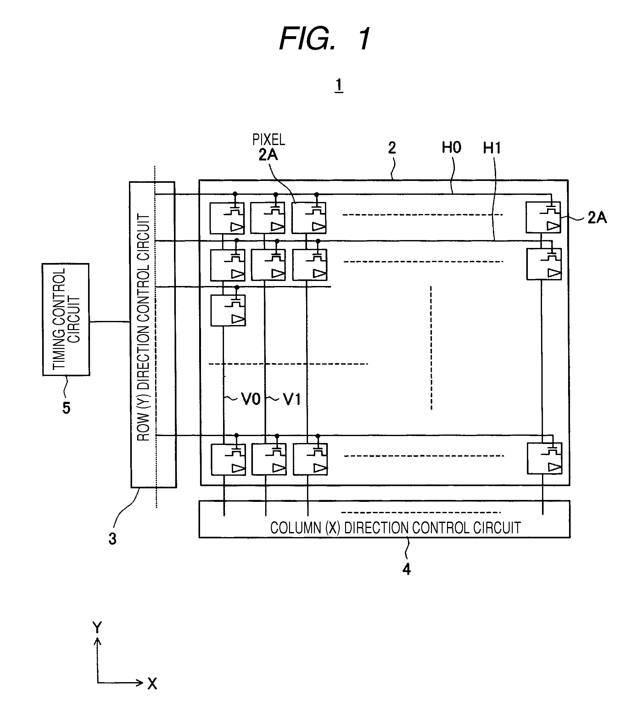
[0102]FIG. 1 is a block diagram of a schematic configuration of a solid-state imaging device according to an embodiment of the present invention.

[0103]A solid-state imaging device 1 includes, as shown in FIG. 1, a pixel section 2 as a sensing section, a row direction (Y-direction) control circuit 3, a column direction (X direction) control circuit 4, and a timing control circuit 5.

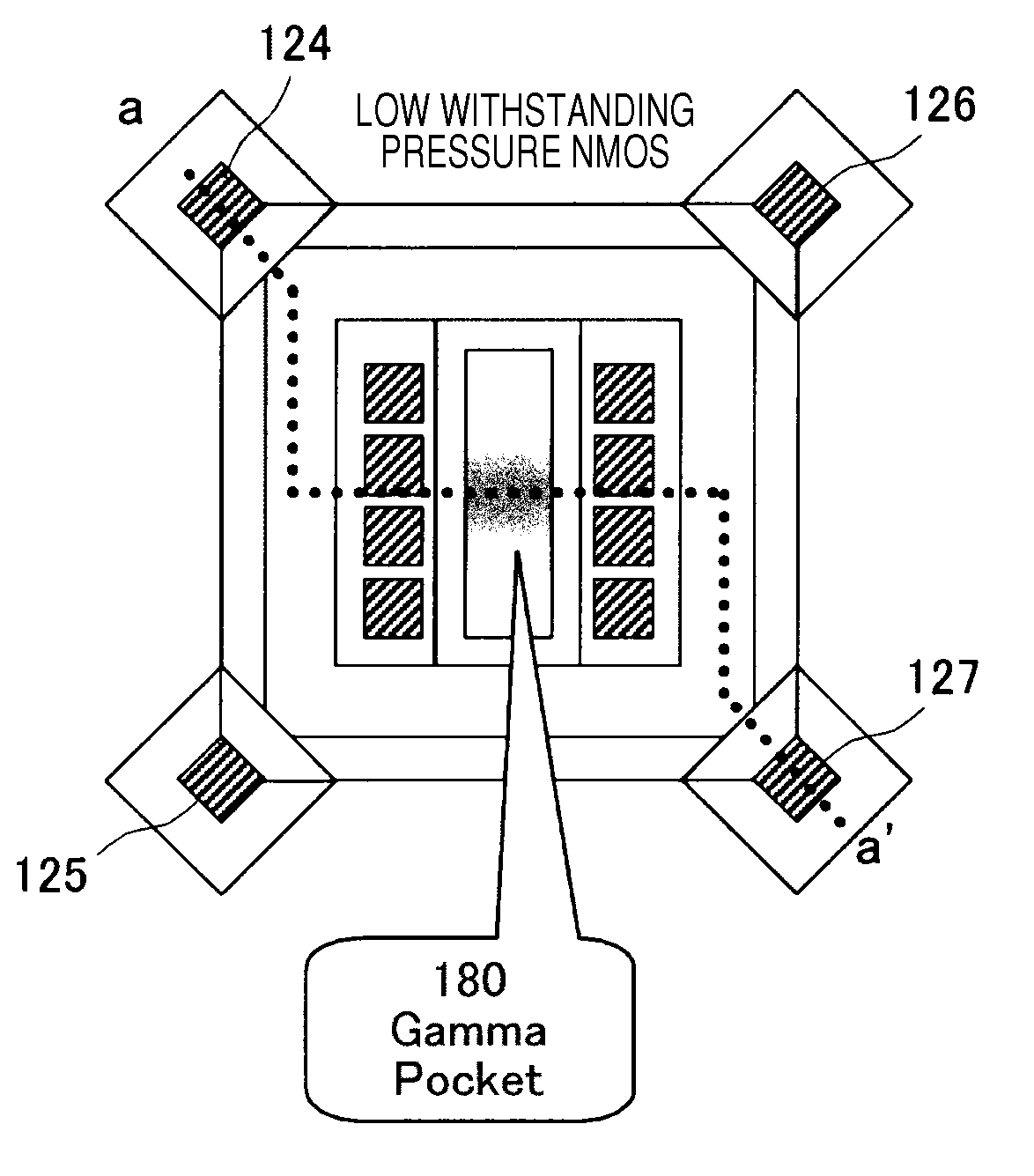
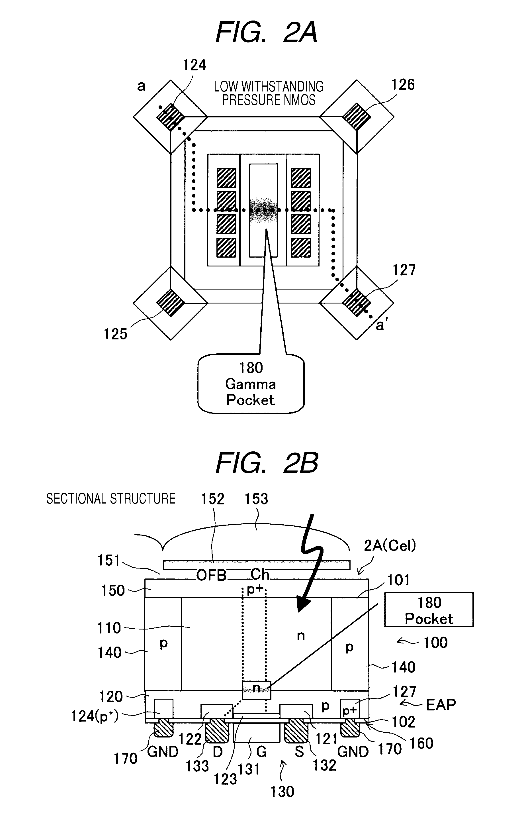
[0104]In the pixel section 2, as described in detail later, plural pixel cells 2A are arranged in, for example, a matrix shape.

[0105]The pixel cells 2A of the pixel section 2 according to this embodiment is configured as a rear (back)-illuminated image sensor of a threshold modulation (CMD) system having the double-well structure.

[0106]The pixel section 2 according to this embodiment adopts the double-well structure. In the pixel section 2, accumulated charges and channel currents are ident...


PUM


Abstract

A solid-state imaging device includes pixel cells that are formed on a substrate having a first substrate surface side, on which light is irradiated, and a second substrate surface side, on which elements are formed, and separated by an adjacent cell group and an element separation layer for each of the pixel cells or with plural pixel cells as a unit. Each of the pixel cells has a first conductive well formed on the first substrate surface side and a second conductive well formed on the second substrate surface side. The first conductive well receives light from the first substrate surface side and has a photoelectric conversion function and a charge accumulation function for the received light. A transistor that detects accumulated charges in the first conductive well and has a threshold modulation function is formed in the second conductive well.

Description

CROSS-REFERENCES TO RELATED APPLICATIONS[0001]The present invention contains subject matter related to Japanese Patent Application JP 2007-326175 filed in the Japanese Patent Office on Dec. 18, 2007, the entire contents of which being incorporated herein by reference.BACKGROUND OF THE INVENTION[0002]1. Field of the Invention[0003]The present invention relates to a solid-state imaging device and a camera having a photoelectric conversion element.[0004]2. Description of the Related Art[0005]It is known that, in solid-state imaging devices such as a CCD image sensor and a CMOS image sensor, a crystal defect in a photodiode as a photoelectric conversion element of a light sensing section and a deep level defect in an interface between the light sensing section and an insulating film thereon cause dark current.[0006]As a method of suppressing the occurrence of the dark currents due to the interface state density, an embedded photodiode structure is effective. The embedded photodiode is c...

Claims


Application Information

Patent Timeline
IPC IPC(8): H04N5/335H04N5/225H01L27/146H04N5/369H04N5/374
CPCH01L27/14621H01L27/14623H01L27/14629H01L27/1463H01L27/1464H01L27/14627
Inventor HIROTA, ISAOHARADA, KOUICHIKARASAWA, NOBUHIROMARUYAMA, YASUSHINITTA, YOSHIKAZUTERAKAGO, HIROYUKITAKASHIMA, HAJIMENOMURA, HIDEO
Owner SONY CORP
Why Eureka
Try Eureka