Asymmetrical RF Drive for Electrode of Plasma Chamber

a plasma chamber and electrode technology, applied in the direction of electric circuits, organic chemistry, manufacturing tools, etc., can solve the problems of undesirable asymmetry in plasma density, and achieve the effect of exacerbated asymmetry and increased plasma density adjacen

Active Publication Date: 2009-06-25
APPLIED MATERIALS INC
View PDF36 Cites 50 Cited by
  • Summary
  • Abstract
  • Description
  • Claims
  • Application Information

AI Technical Summary

Benefits of technology

[0016]The invention is counter-intuitive because one might expect that positioning the RF power drive points closer to the workpiece passageway would further increase the plasma density adjacent the passageway and thereby exacerbate the asymmetry in plasma density. However, we have found that the opposite is true, as explained below.

Problems solved by technology

The asymmetry in plasma density is undesirable because it produces a corresponding asymmetry in the plasma process (e.g., deposition or etch) being performed on the workpiece.

Method used


Image

  • Asymmetrical RF Drive for Electrode of Plasma Chamber
  • Asymmetrical RF Drive for Electrode of Plasma Chamber
  • Asymmetrical RF Drive for Electrode of Plasma Chamber

Examples


Embodiment Construction

1. Plasma Chamber Overview

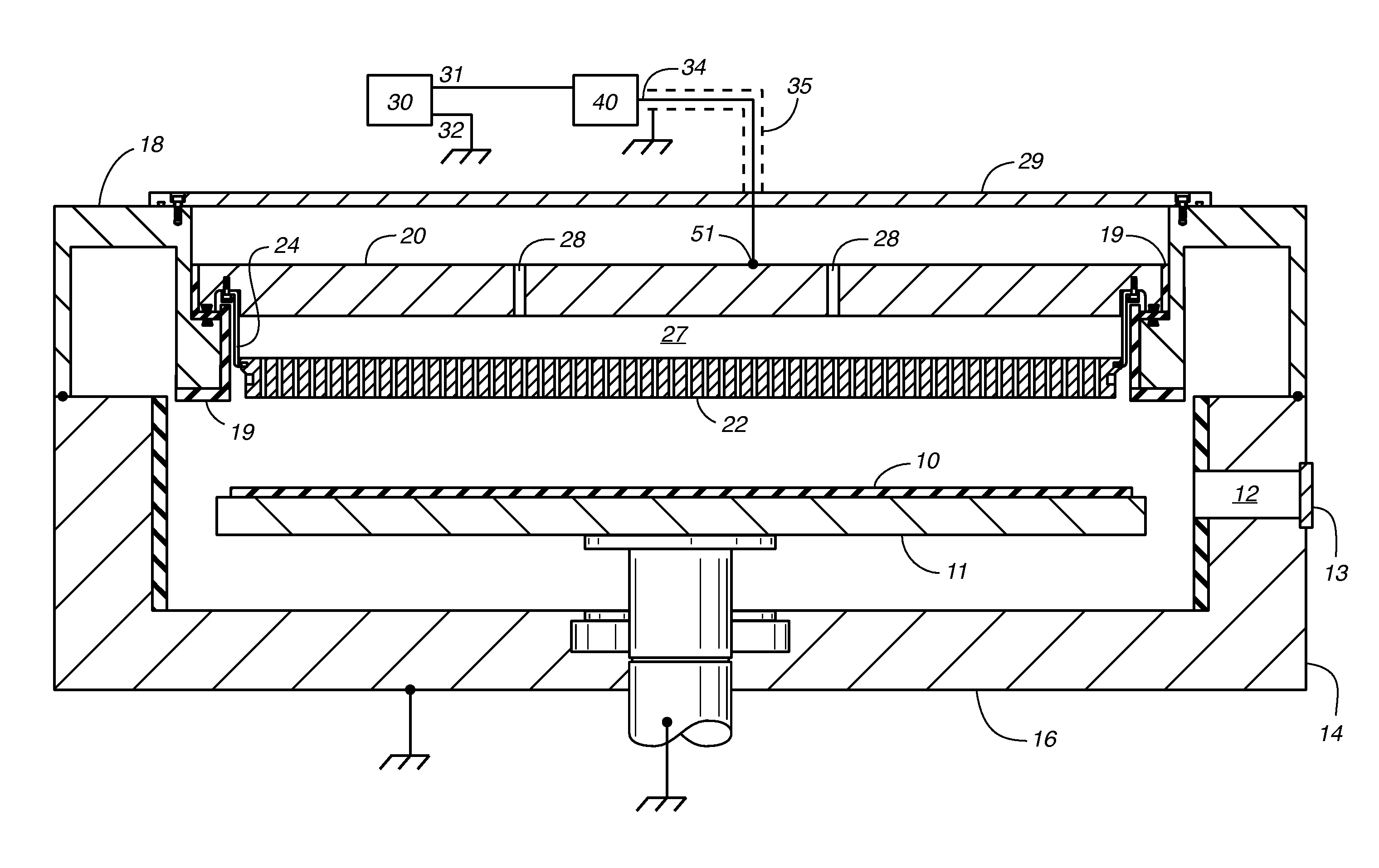
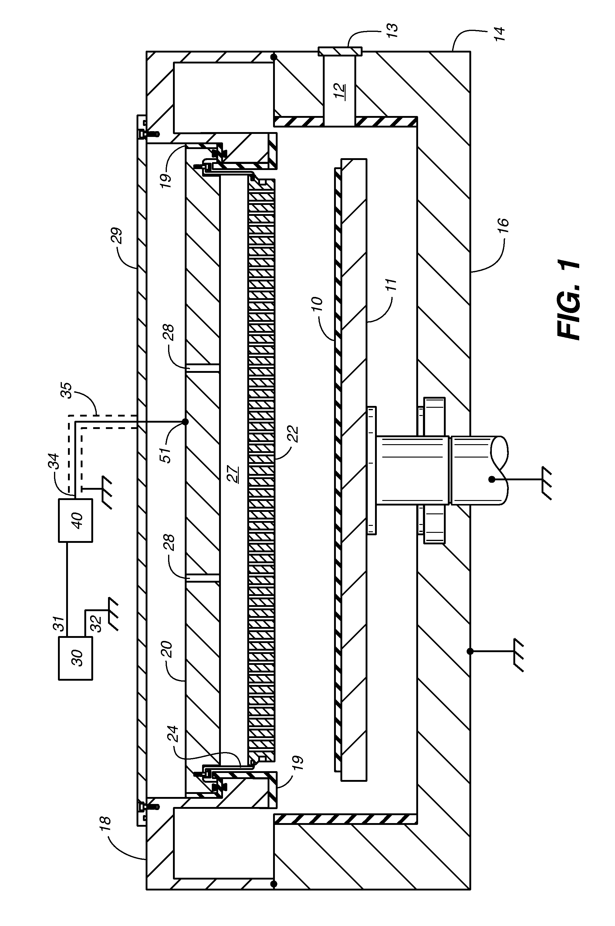
[0025]FIG. 1 shows a plasma chamber that includes one embodiment of the invention. Before describing the invention, the conventional components of the plasma chamber will be described.

[0026]The plasma chamber is intended to subject a workpiece 10 to a plasma process step for fabricating on the workpiece electronic devices such as semiconductor devices, a display, or solar cells. The workpiece is supported within the chamber by a workpiece support 11, also called a chuck or susceptor. Examples of a workpiece 10 that would be processed within the plasma chamber include a rectangular glass substrate on which flat panel displays are fabricated or a circular semiconductor wafer on which integrated circuits are fabricated.

[0027]The plasma chamber has a chamber wall 14-20 that provides a vacuum enclosure for the chamber interior. In the illustrated embodiment, the chamber side wall 14 and chamber bottom wall 16 are implemented as a unitary wall. The top of the cha...


PUM

PropertyMeasurementUnit
RF poweraaaaaaaaaa
electrical poweraaaaaaaaaa
timeaaaaaaaaaa

Abstract

RF power is coupled to one or more RF drive points (50-56) on an electrode (20-28) of a plasma chamber such that the level of RF power coupled to the RF drive points (51-52, 55-56) on the half (61) of the electrode that is closer to the workpiece passageway (12) exceeds the level of RF power coupled to the RF drive points (53-54), if any, on the other half (62) of the electrode. Alternatively, RF power is coupled to one or more RF drive points on an electrode of a plasma chamber such that the weighted mean of the drive point positions is between the center (60) of the electrode and the workpiece passageway. The weighted mean is based on weighting each drive point position by the time-averaged level of RF power coupled to that drive point position. The invention offsets an increase in plasma density that otherwise would exist adjacent the end of the electrode closest to the passageway.

Description

CROSS REFERENCE TO RELATED APPLICATION[0001]This patent application claims the benefit of U.S. Provisional Application No. 61 / 016,592 filed Dec. 25, 2007.FIELD OF THE INVENTION[0002]The invention relates generally to coupling an RF power source to an electrode of a plasma chamber used for fabricating electronic devices such as semiconductors, displays and solar cells. The invention relates more specifically to improving the uniformity of a plasma process performed in the chamber by coupling such RF power source to the electrode asymmetrically so as to offset asymmetry in the chamber geometry.BACKGROUND OF THE INVENTION[0003]Plasma chambers commonly are used to perform processes for fabricating electronic devices such as semiconductors, displays and solar cells. Such plasma fabrication processes include chemical vapor deposition of semiconductor, conductor or dielectric layers on the surface of a workpiece or etching of selected portions of such layers on the workpiece surface.[0004]...

Claims


Application Information

Patent Timeline
Patent Type & Authority Applications(United States)
IPC IPC(8): H05H1/00H01L21/3065B23H7/14
CPCH01J37/32091H01J37/32577H01L21/02104C23C16/513H01L21/02B44C1/227H01J37/32174
Inventor KUDELA, JOZEFSORENSEN, CARL A.CHOI, SOO YOUNGWHITE, JOHN M.
Owner APPLIED MATERIALS INC
Why Eureka
Try Eureka