Nonvolatile semiconductor memory device and method of fabricating the same

a semiconductor memory and non-volatile technology, applied in the direction of semiconductor devices, basic electric elements, electrical appliances, etc., can solve the problems of non-uniform electric field being created in the device, loss of stored data of volatile memory devices, interference between cells, etc., and achieve the effect of improving the reliability of the devi

Inactive Publication Date: 2009-06-25
SAMSUNG ELECTRONICS CO LTD
View PDF3 Cites 6 Cited by
  • Summary
  • Abstract
  • Description
  • Claims
  • Application Information

AI Technical Summary

Benefits of technology

[0011]The invention provides a memory cell structure and method of manufacturing the memory cell structure in which the trapping of electrons at the edges of the active region, i.e., the edge effect, is substantially reduced or eliminated. As a result, after programming of the devices, the threshold voltages of the programmed cells are substantially uniform throughout the cells. This results in improved reliability of the devices.

Problems solved by technology

Volatile memory devices lose their stored data when power to the devices is interrupted or discontinued.
This results in a non-uniform electric field being created in the device, that is, the electric field is higher at the edge of the active region than at other parts of the active region.
This is commonly referred to as the “edge effect,” in which non-uniform collections of trapped electrons at edges of the active regions cause interference between cells and degrade the operation of the device.
As a result of the edge effect in which the uneven trapping of electrons occurs, devices in the programmed device have non-uniform threshold voltages Vth.
Errors may occur during the programming of cells.
This results in a degradation of the overall operation of the memory device.

Method used


Image

  • Nonvolatile semiconductor memory device and method of fabricating the same
  • Nonvolatile semiconductor memory device and method of fabricating the same
  • Nonvolatile semiconductor memory device and method of fabricating the same

Examples


Embodiment Construction

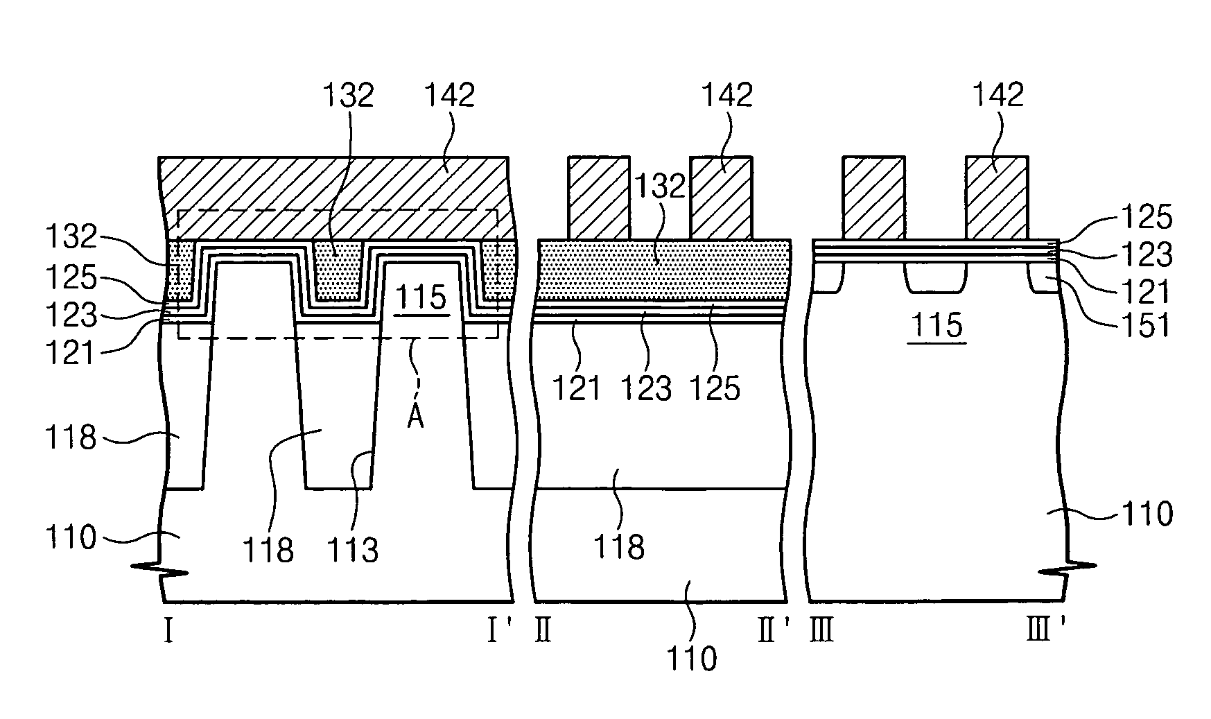
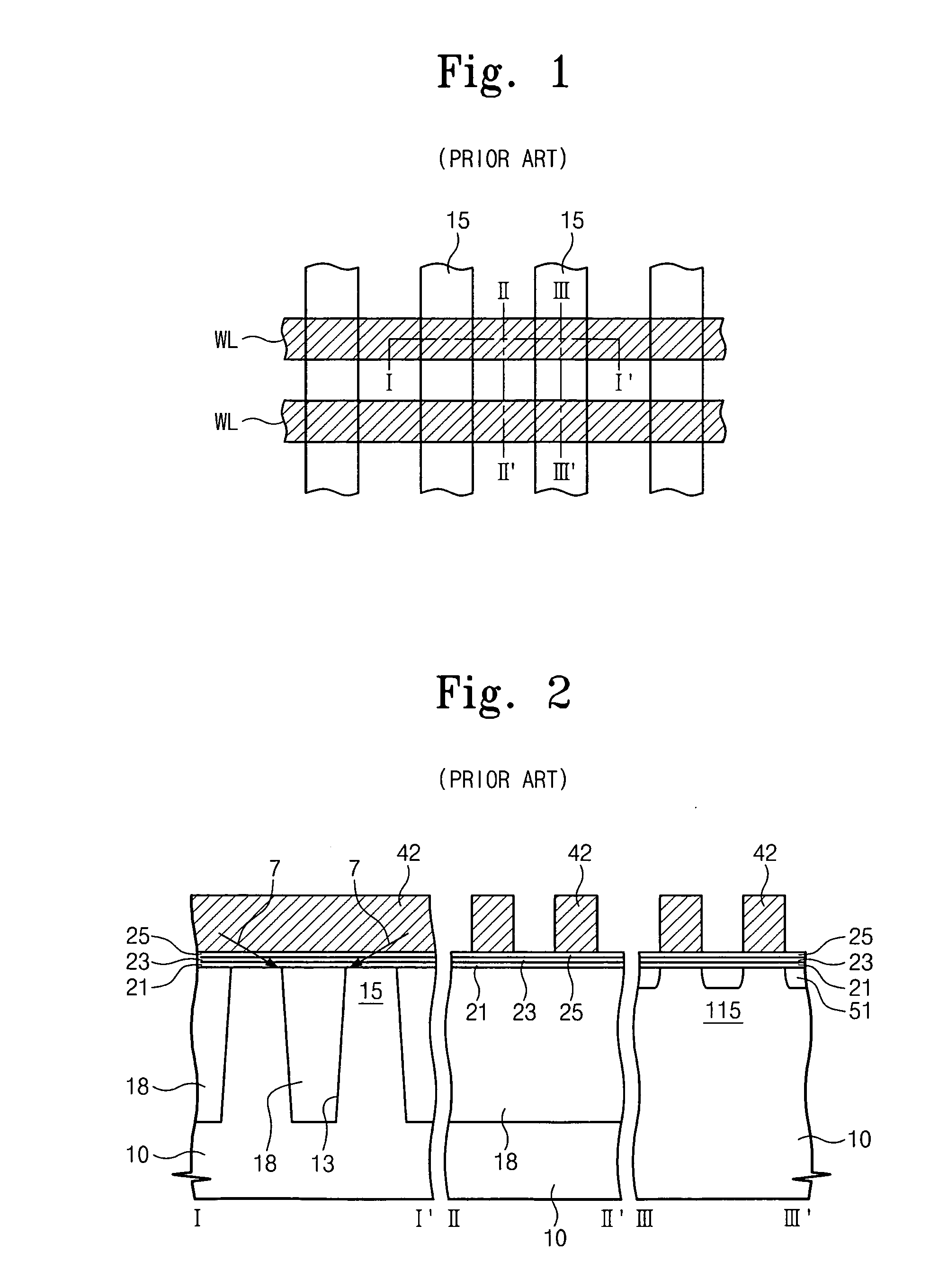
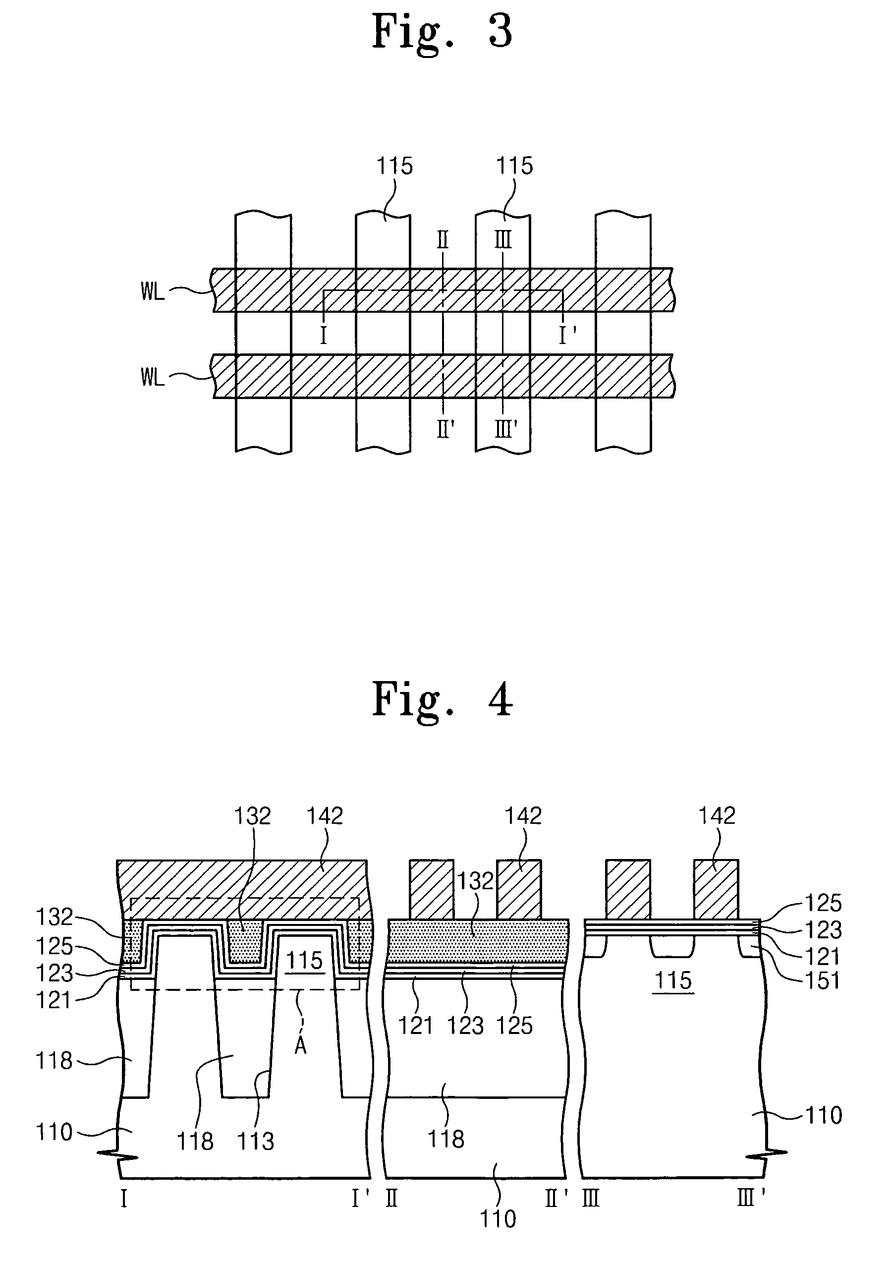
[0039]According to the invention, the trapping of electrons at the edge of the active region of memory cells is substantially reduced or eliminated. This is realized by including a resistance region, layer or pattern over the blocking layer and the STI, but not over the active region. The resistance layer blocks the lateral or oblique flow of electrons, as shown by the arrows 7 in FIG. 2 for conventional devices, such that, in the device of the invention, electrons are not non-uniformly trapped at the edge of the active region. Threshold voltages of cells are uniform, resulting in improved operational characteristics and reliability of the devices.

[0040]FIG. 3 contains a schematic plan view of a memory device using a floating-trap memory structure with a resistance pattern or layer according to the present invention. FIG. 4 contains three schematic cross-sectional views of the floating-trap memory structure of FIG. 3, according to one embodiment of the invention. The three schematic...


PUM


Abstract

A charge trap flash (CTF) memory cell and manufacturing method include a semiconductor substrate and an isolation region and an active region being formed in the substrate. A tunneling layer, a charge trapping layer and a blocking layer are formed on the isolation region and the active region. A resistance layer is formed on the blocking layer over the isolation region. The resistance layer prevents or substantially reduces trapping of electrons at the edges of the active region, i.e., the edge effect. As a result, after programming of the devices, the threshold voltages of the programmed cells are substantially uniform throughout the cells. This results in improved reliability of the devices.

Description

RELATED APPLICATION[0001]This application claims priority to Korean Patent Application number 10-2007-0135386, filed in the Korean Intellectual Property Office on Dec. 21, 2007, the entire contents of which are incorporated herein by reference.BACKGROUND OF THE INVENTION[0002]1. Field of the Invention[0003]This application relates to semiconductor memory devices and methods of manufacturing semiconductor memory devices. In particular, this application relates to a charge trap flash (CTF) memory cell with an edge SANOS (silicon-aluminum oxide-nitride-oxide-silicon) structure and a method of manufacturing the CTF memory cell.[0004]2. Discussion of the Related Art[0005]Semiconductor memory devices are widely used to store data in electronic systems. Memory devices are generally classified as either volatile or non-volatile devices. Volatile memory devices lose their stored data when power to the devices is interrupted or discontinued. Non-volatile memory devices retain their data when ...

Claims


Application Information

Patent Timeline
Patent Type & Authority Applications(United States)
IPC IPC(8): H01L29/792
CPCH01L27/11565H01L29/792H01L27/11568H10B43/10H10B43/30H01L21/76224H01L21/76838
Inventor PARK, JIN-TAEKCHOI, JUNGDAL
Owner SAMSUNG ELECTRONICS CO LTD
Why Eureka
Try Eureka