Substrate treating apparatus, substrate treating method, and method for manufacturing high-voltage device

a substrate treatment and substrate technology, applied in the manufacture of electrode systems, electric discharge tubes/lamps, tube/lamp factory adjustment, etc., can solve the problems of s/n, ion gage monitoring a vacuum state cannot be used, and it is extremely difficult to distinguish discharge from light emission, so as to achieve accurate detection of adhesion

Inactive Publication Date: 2009-06-25
CANON KK
View PDF0 Cites 0 Cited by
  • Summary
  • Abstract
  • Description
  • Claims
  • Application Information

AI Technical Summary

Benefits of technology

[0010]An object of the present invention is to provide a technique for accurately detecting adhesion and deposition of undesired substances onto a treatment electrode in order to perform a normal withstand voltage treatment.

Problems solved by technology

Namely, in the prior art, low light is detected, and therefore, stray light or light emission due to other than discharge remarkably reduces sensitivity (S / N).
Additionally, an ion gage for monitoring a vacuum state cannot be used because a detection line emits light.
Further, when metastable light emission due to contact resistance occurs at a contact point between a contact for supplying a voltage to the target substrate and the target substrate, it is extremely difficult to distinguish discharge from the light emission.
Thus, there is a problem that it is very difficult to suppress the entering and generation of light caused by other than discharge, and the sensitivity required for monitoring of discharge cannot be ensured.
However, since the minute amount of the electrical signal is output, the S / N is poor, whereby it is difficult to perform the detection with high accuracy.
In addition, in these methods, the accidental movement of fine particles, that is, a pulsed electrical signal is detected, and thus, it is impossible to detect a field emission current like DC generated from undesired substances adhered onto the treatment electrode surface.
Thus, a minute current flows according to this transfer; however, in the case (1), since the peeling of undesired substances does not reduce the function of the substrate, the minute current is not measured.
Meanwhile, in the case (2), the function of the substrate is reduced, and, at the same time, the peeling from the peeling part is repeatedly continued, and therefore, even if the withstand voltage treatment is applied to the substrate, the withstand voltage cannot be guaranteed.
The normal withstand voltage treatment may not be performed when undesired substances are deposited on the treatment electrode other than when the target substrate itself has a problem.
Thus, the normal withstand voltage treatment cannot be performed in such a region.

Method used


Image

  • Substrate treating apparatus, substrate treating method, and method for manufacturing high-voltage device
  • Substrate treating apparatus, substrate treating method, and method for manufacturing high-voltage device
  • Substrate treating apparatus, substrate treating method, and method for manufacturing high-voltage device

Examples


first embodiment

Substrate Treating Apparatus of First Embodiment

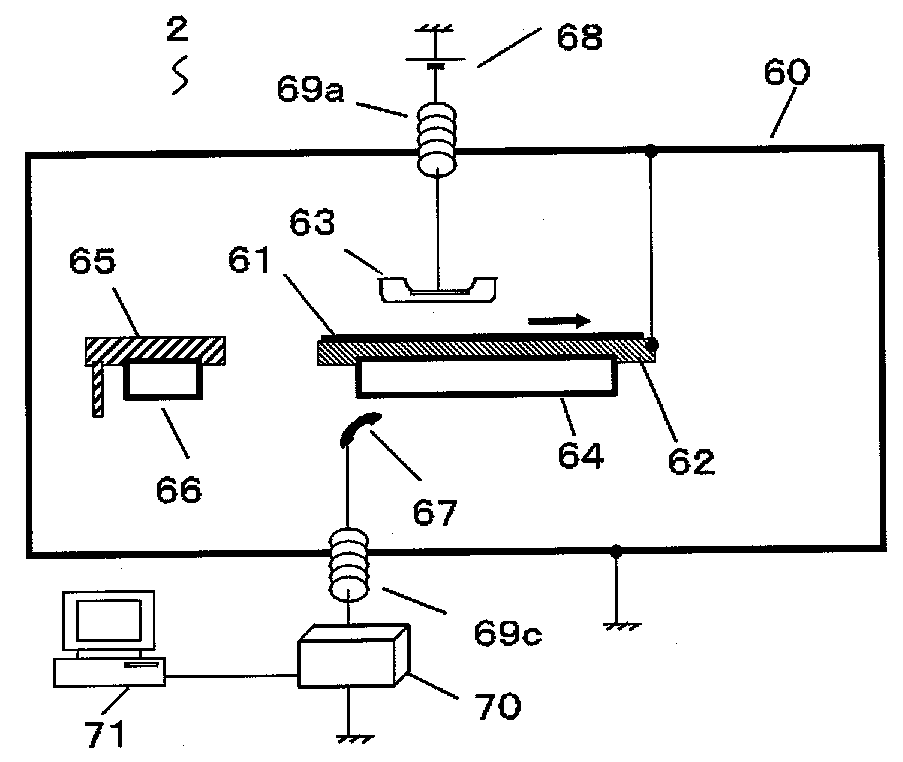
[0035]The first embodiment of this invention is described. FIG. 3 is a view showing a structural example of a substrate treating apparatus 2 according to the first embodiment. In FIG. 3, the substrate treating apparatus 2 has a vacuum treatment bath (vacuum chamber) 60. The vacuum treatment bath 60 includes a rectangular plate-like substrate holding part (substrate holding unit) 62 on which a substrate (target substrate) 61, which is a target to be treated, that is, a target to be monitored, is placed. The vacuum treatment bath 60 further includes a rectangular plate-like treatment electrode 63 provided so as to be opposed to the substrate holding part 62. The plane area of the treatment electrode 63 is smaller than the plane area of the substrate 61. In the present embodiment, for example, the width of the treatment electrode 63 (dimension in the direction vertical to the drawing in FIG. 3) is somewhat larger than the width of the sub...

second embodiment

Substrate Treating Apparatus of Second Embodiment

[0054]A substrate treating apparatus of a second embodiment has abnormality detecting unit for detecting the abnormality in the substrate treatment (withstand voltage treatment). Other constitutions are substantially the same as the constitutions of the first embodiment. Hereinafter, an abnormality detecting method in the prior art substrate treating apparatus is first described as a comparative example, and thereafter, an abnormality detecting method in the present embodiment is described.

(Prior Art Abnormality Detecting Method)

[0055]FIG. 5 shows a constitution of the prior art substrate treating apparatus.

[0056]As shown in FIG. 5, a substrate treating apparatus 30 has a vacuum chamber 32 operating as a vacuum treatment bath and an exhaust device 33 for evacuating inside the vacuum treatment bath. A rectangular plate-like substrate placement part 36 on which a substrate 34 to be treated or monitored is placed and a rectangular plate-...


PUM

PropertyMeasurementUnit
electric currentaaaaaaaaaa
thicknessaaaaaaaaaa
anode voltageaaaaaaaaaa

Abstract

A substrate treating apparatus, in which a voltage is applied to between a treatment electrode and a target substrate in such a state that the treatment electrode is opposed to the target substrate to thereby perform substrate treatment for removing undesired substances on the target substrate, has a reference electrode, a transfer unit which transfers at least one of the treatment electrode and the reference electrode to thereby provide the treatment electrode so that the treatment electrode is opposed to the reference electrode, and a check unit for applying a voltage to between the treatment electrode and the reference electrode in such a state that the treatment electrode is opposed to the reference electrode and thereby checking an adhesion level of undesired substances onto the treatment electrode surface.

Description

BACKGROUND OF THE INVENTION[0001]1. Field of the Invention[0002]The present invention relates to a substrate treating apparatus, which treats a substrate constituting an image display apparatus, and a substrate treating method. The present invention further relates to a method for manufacturing a high-voltage device.[0003]2. Description of the Related Art[0004]Recently, various types of flat type image display apparatuses have attracted attention as a next-generation light and thin image display apparatus to replace a cathode-ray tube (hereinafter referred to as a CRT). For example, there has been known a plasma display (PDP) using luminescence of a phosphor due to a discharge phenomenon, a liquid crystal display (LCD), and a display using an electron-emitting device such as a filed emission device and a surface-conduction electron-emitting device.[0005]In general, the display using the electron-emitting device uses a rear plate with the electron-emitting device disposed thereon and...

Claims


Application Information

Patent Timeline
Patent Type & Authority Applications(United States)
IPC IPC(8): H01J9/00
CPCH01J9/38H01J31/127H01J9/42
Inventor KOIDE, SATOSHIISEKI, YASUSHIISHII, AKIRA
Owner CANON KK
Why Eureka
Try Eureka