Photosensitive microelectronic device with avalanche multipliers

a microelectronic device and avalanche multiplier technology, applied in the field of microelectronic imaging or image sensor devices, can solve the problems of awkward pixel formation provided with amplification means, incompatibility of arrays with low voltage avalanche operation, and difficulty in reducing the size of pixels

Inactive Publication Date: 2009-07-02
COMMISSARIAT A LENERGIE ATOMIQUE ET AUX ENERGIES ALTERNATIVES
View PDF9 Cites 8 Cited by
  • Summary
  • Abstract
  • Description
  • Claims
  • Application Information

AI Technical Summary

Problems solved by technology

In order to minimise the losses, important production constraints, for example such as the doping of the substrate on which the array is formed, are provided for, and render these arrays incompatible with a low voltage avalanche operation.
However, the formation of pixels provided with amplification means is awkward.
The formation of an array of avalanche photodiodes is known but poses numerous problems, such as the necessity of a high voltage supply, typically around 70V, and that of a cooling system.
Moreover, with such a device, it is difficult to reduce the size of the pixels.
Such an architecture is disclo...

Method used


Image

  • Photosensitive microelectronic device with avalanche multipliers
  • Photosensitive microelectronic device with avalanche multipliers
  • Photosensitive microelectronic device with avalanche multipliers

Examples


Embodiment Construction

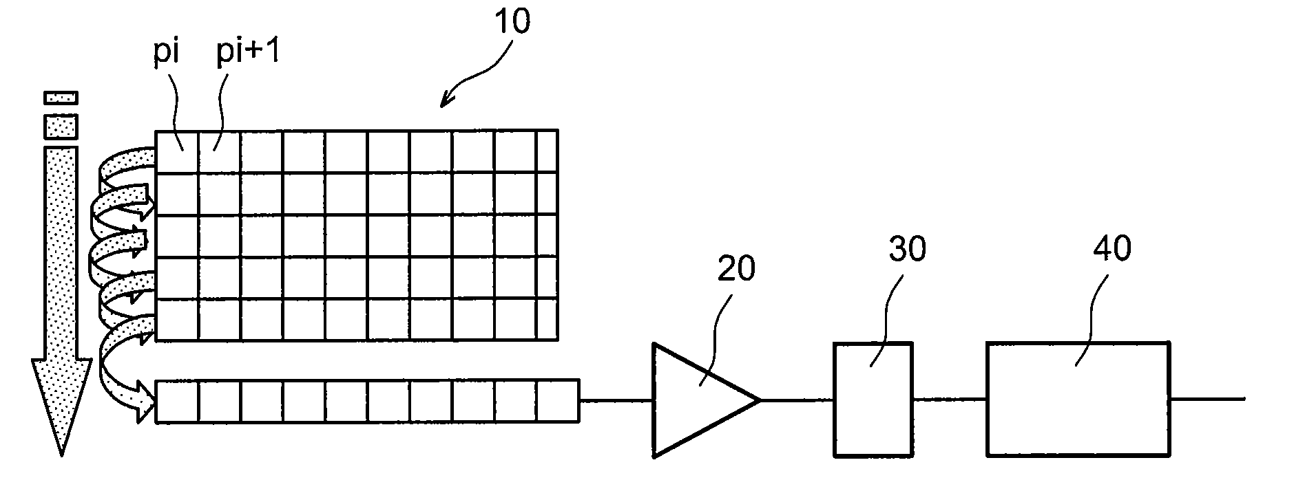
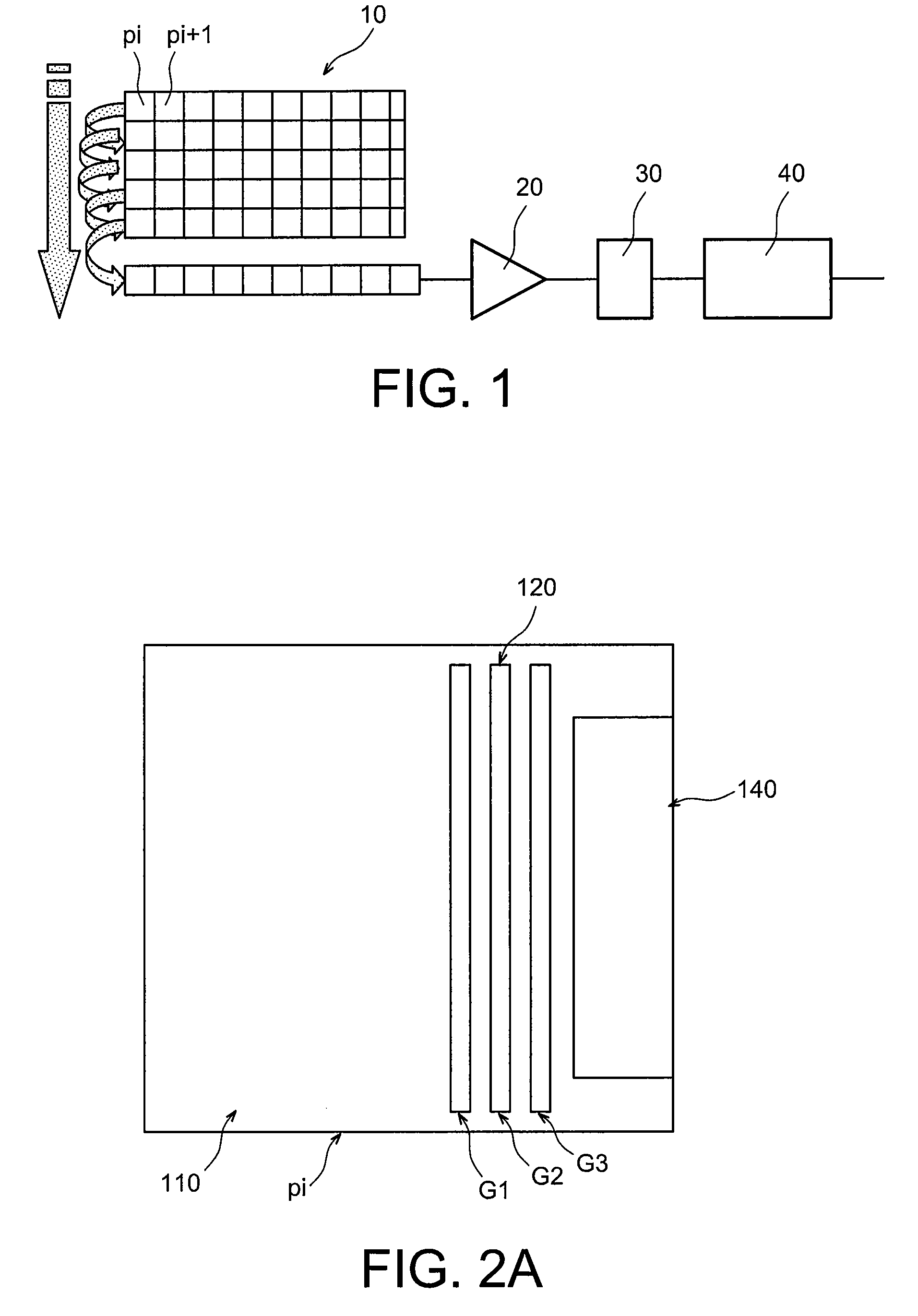
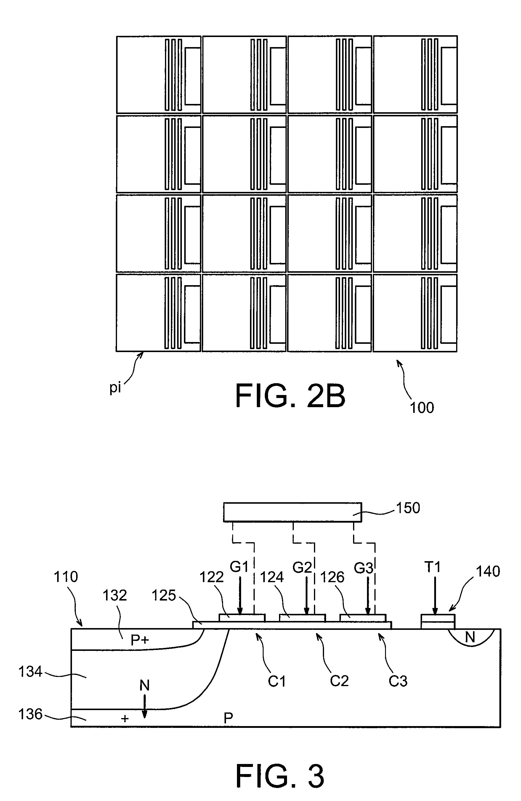
[0016]The invention concerns a photosensitive microelectronic detector device, in particular an array of image sensors, comprising several elementary cells or several elementary pixels, at least several elementary cells comprising:[0017]at least one photosensitive zone for capturing photon(s) and converting photon(s) into electron(s),[0018]multiplier means, provided to produce, by electronic avalanche or ionisation by impact, during cycle(s) known as electron “multiplication” cycles, a higher number of electrons than the number of electrons converted by the photosensitive zone, the multiplier means comprising at least one plurality of electrodes of control gates, opposite at least one semi-conducting zone.

[0019]At least one control circuit of said gates may be provided to apply control signals respectively to said control gates.

[0020]During the multiplication cycle(s), the multiplier means may have a given, desired gain, which may be adapted by the control circuit.

[0021]The gates of...


PUM


Abstract

Microelectronic image sensor array device comprising a plurality of elementary cells laid out according to an array and each provided with at least one photosensitive zone for capturing photon(s) and converting photon(s) into electron(s), at least one or several of said cells comprising electronic avalanche multiplier means, provided to produce, during cycles known as electron amplification cycles, a greater number of electrons than the number of electrons converted by the photosensitive zone, the device further comprising a control circuit adapted to modulate the amplification gain of each cell individually.

Description

TECHNICAL FIELD[0001]The present invention relates to the field of microelectronic imaging or image sensor devices, in particular in CMOS technology.[0002]The invention concerns a photosensitive microelectronic device as well as an image sensor provided with pixels formed of a photosensitive microelectronic device comprising a photosensitive zone associated with means for multiplying electrons by electronic avalanche comprising a plurality of control gates.[0003]The invention brings improvements, particularly in terms of gain and sensitivity compared to conventional CMOS arrays, while making it possible to operate with a supply voltage less than that of CCD arrays according to the prior art.[0004]The invention also brings improvements in terms of image dynamic.STATE OF THE PRIOR ART[0005]Generally it is aimed to integrate a greater and greater number of pixels within CMOS (complementary metal oxide semiconductor) or CCD (charge coupled device) type imaging devices. Consequently, the...

Claims


Application Information

Patent Timeline
IPC IPC(8): H04N5/335H04N5/3745
CPCH01L27/14609H01L27/14643H04N5/3745H04N3/155H01L31/107H04N25/77
Inventor CARRIERE, NICOLAS
Owner COMMISSARIAT A LENERGIE ATOMIQUE ET AUX ENERGIES ALTERNATIVES
Why Eureka
Try Eureka