Method of Forming Isolation Layer of Semiconductor Device

a technology of isolation layer and semiconductor, which is applied in the direction of semiconductor/solid-state device manufacturing, electrical equipment, basic electric elements, etc., can solve the problems of large leakage current, crystalline defects in silicon substrates, and reduced effective area of source/drain regions, so as to prevent mechanical stress and electrical stress

Inactive Publication Date: 2009-07-02
SK HYNIX INC
View PDF4 Cites 13 Cited by
  • Summary
  • Abstract
  • Description
  • Claims
  • Application Information

AI Technical Summary

Benefits of technology

[0007]The invention is directed to prevent mechanical stress and electrical stress from being concentrated on both ends of a tunnel dielectric layer by making each of the both ends of the tunnel dielectric layer, having a pointed profile, a round profile through an O2 plasma process.

Problems solved by technology

However, the LOCOS method is disadvantageous in that a bird's beak occurs due to lateral oxidization, which as a result widens the isolation region, and the sizes of the effective areas of source / drain regions can be reduced.
The LOCOS method is also disadvantageous in that crystalline defects are generated in the silicon substrate because stress due to a difference in the coefficient of thermal expansion is concentrated on the corners of the oxide layer when the field oxide layer is formed and, therefore, the leakage current is large.
Accordingly, typical isolation methods, such as LOCOS, have reached their limits.

Method used


Image

  • Method of Forming Isolation Layer of Semiconductor Device
  • Method of Forming Isolation Layer of Semiconductor Device
  • Method of Forming Isolation Layer of Semiconductor Device

Examples


Embodiment Construction

[0013]A specific embodiment according to the invention is described below with reference to the accompanying drawings. However, the invention is not limited to the disclosed embodiment, but may be implemented in various ways. The embodiment is provided to complete the disclosure of the invention and to allow those having ordinary skill in the art to understand the scope of the invention. The scope of the invention is defined by the claims.

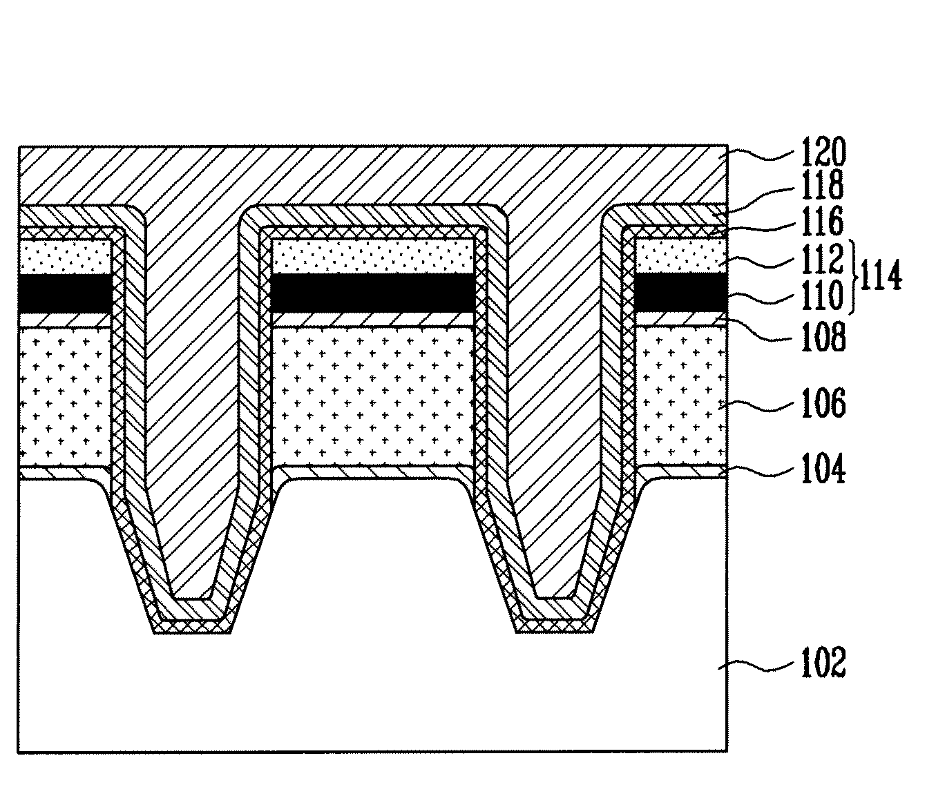
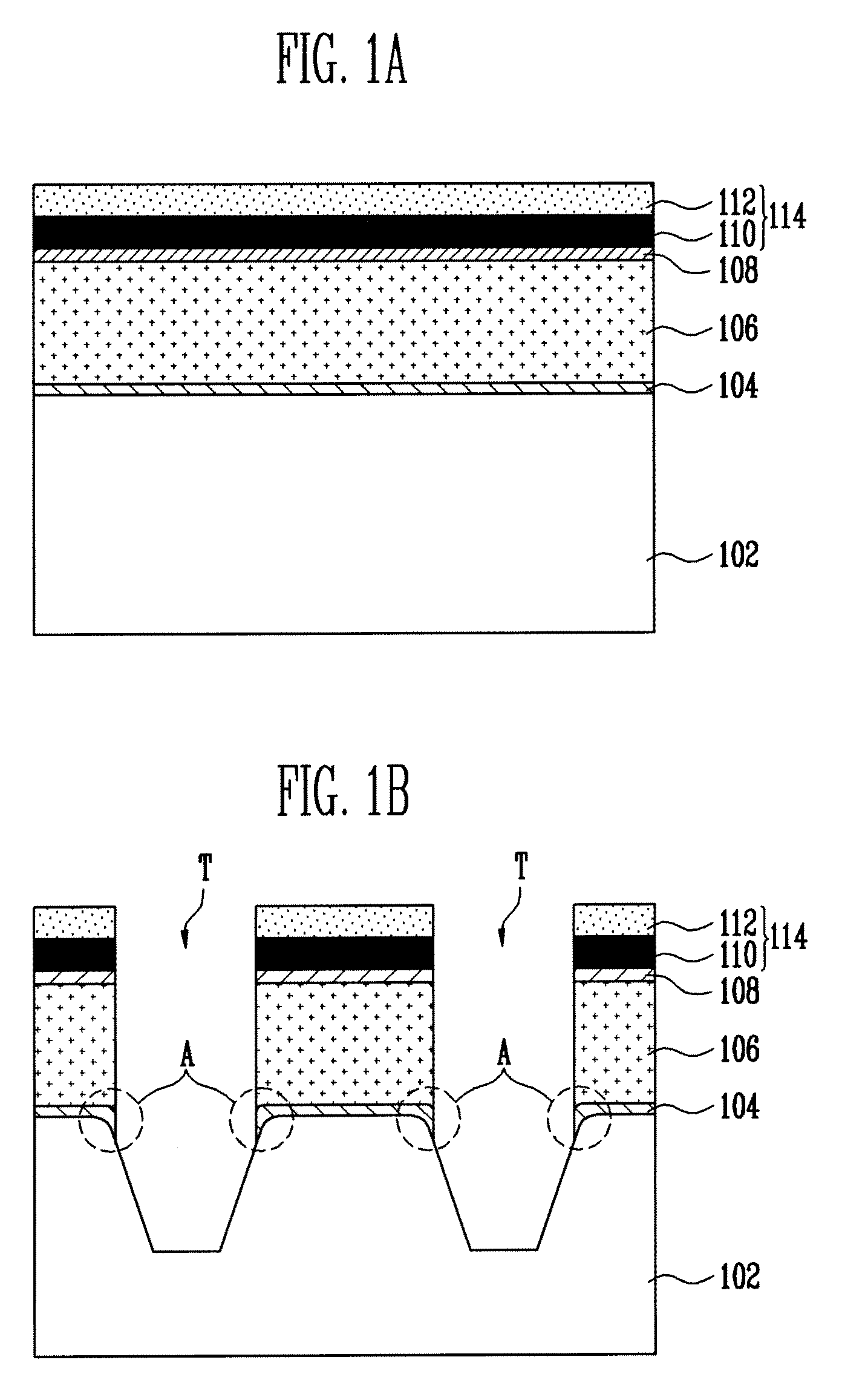
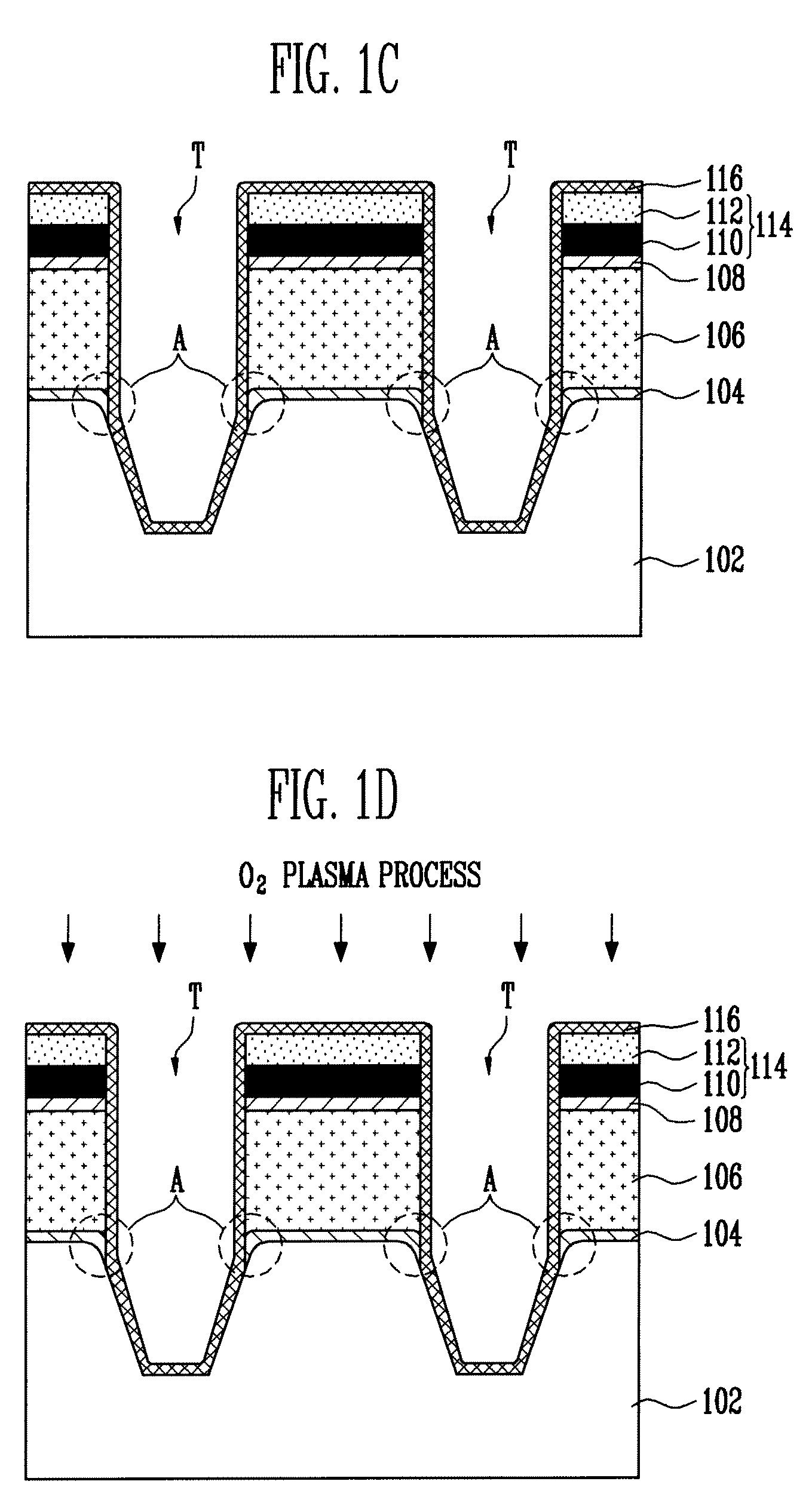
[0014]FIGS. 1A to 1F are cross-sectional views a method of forming isolation layers of a semiconductor device in accordance with the invention.

[0015]Referring to FIG. 1A, a screen oxide layer (not shown) is formed on a semiconductor substrate 102. A well ion implantation process or a threshold voltage ion implantation process is performed on the semiconductor substrate 102. The well ion implantation process is performed to form a well region in the semiconductor substrate 102. The threshold voltage ion implantation process is performed to control t...


PUM


Abstract

A method of forming isolation layers of a semiconductor device, comprising providing a semiconductor substrate in which a tunnel dielectric layer and a conductive layer are formed in active regions having two ends and trenches are formed in isolation regions; rounding both ends of each active region by performing an O2 plasma process on the semiconductor substrate; forming a first insulating layer on sidewalls of each trench; and, forming a second insulating layer, preferably having a greater fluidity than that of the first insulating layer, on the first insulating layer.

Description

CROSS-REFERENCE TO RELATED APPLICATION[0001]Priority to Korean patent application number 10-2007-0138815, filed on Dec. 27, 2007, the disclosure of which is incorporated by reference in its entirety, is claimed.BACKGROUND OF THE INVENTION[0002]The invention relates generally to a method of forming isolation layers of a semiconductor device and, more particularly, to a method of forming isolation layers of a semiconductor device, which can form the isolation layers in an isolation region of a substrate by employing a shallow trench isolation (STI) process.[0003]Generally, a semiconductor device formed in a silicon wafer includes isolation regions for electrically isolating semiconductor elements. In particular, with the high degree of integration and miniaturization of semiconductor devices, active research has been done on size reduction of individual elements and also of the isolation region, since the process of forming the isolation regions is an initial process step of the entir...

Claims


Application Information

Patent Timeline
Patent Type & Authority Applications(United States)
IPC IPC(8): H01L21/762
CPCH01L21/76232H01L21/76
Inventor PARK, BO MIN
Owner SK HYNIX INC
Why Eureka
Try Eureka