[0042]According to the technique of
Patent Document 1, the precharge / predischarge circuit 120 which is an analog
amplifier carries out writing during the precharge / predischarge periods so as to raise a node potential to around a desired reference potential and then directly writes the reference potential by the output circuit 100 whose current supplying ability is suppressed, thereby removing the
error factor such as the offset voltage and the like of the analog
amplifier. However, such control is carried out in a time-divisional manner with predetermined time intervals such as t1-t0, t2-t1, and the like, which raises such problem that this technique is less applicable and less versatile with respect to
process variation. For example, in case of applying the arrangement of
Patent Document 1 to a data
signal line driving circuit of a
liquid crystal display device, a load of a data signal line which should be driven is arbitrarily determined depending on a panel size, a structure of pixels to be connected,
liquid crystal material to be used, and a similar factor. Further, also properties of a TFT to be driven have predetermined unevenness. In this manner, the load varies depending on the structure condition and the process condition. In case of the arrangement of
Patent Document 1, it is necessary to realize a circuit and a timing each of which covers entire (or partial) conditions, or it is necessary to realize a circuit and a timing each of which is optimized for each condition. The former arrangement increases the
power consumption due to its excessive driving ability, and the latter arrangement increases time taken to design a circuit and to carry out trial production thereof.
[0043]The analog circuit of Patent Document 2 does not have a
constant current source, so that this results in such
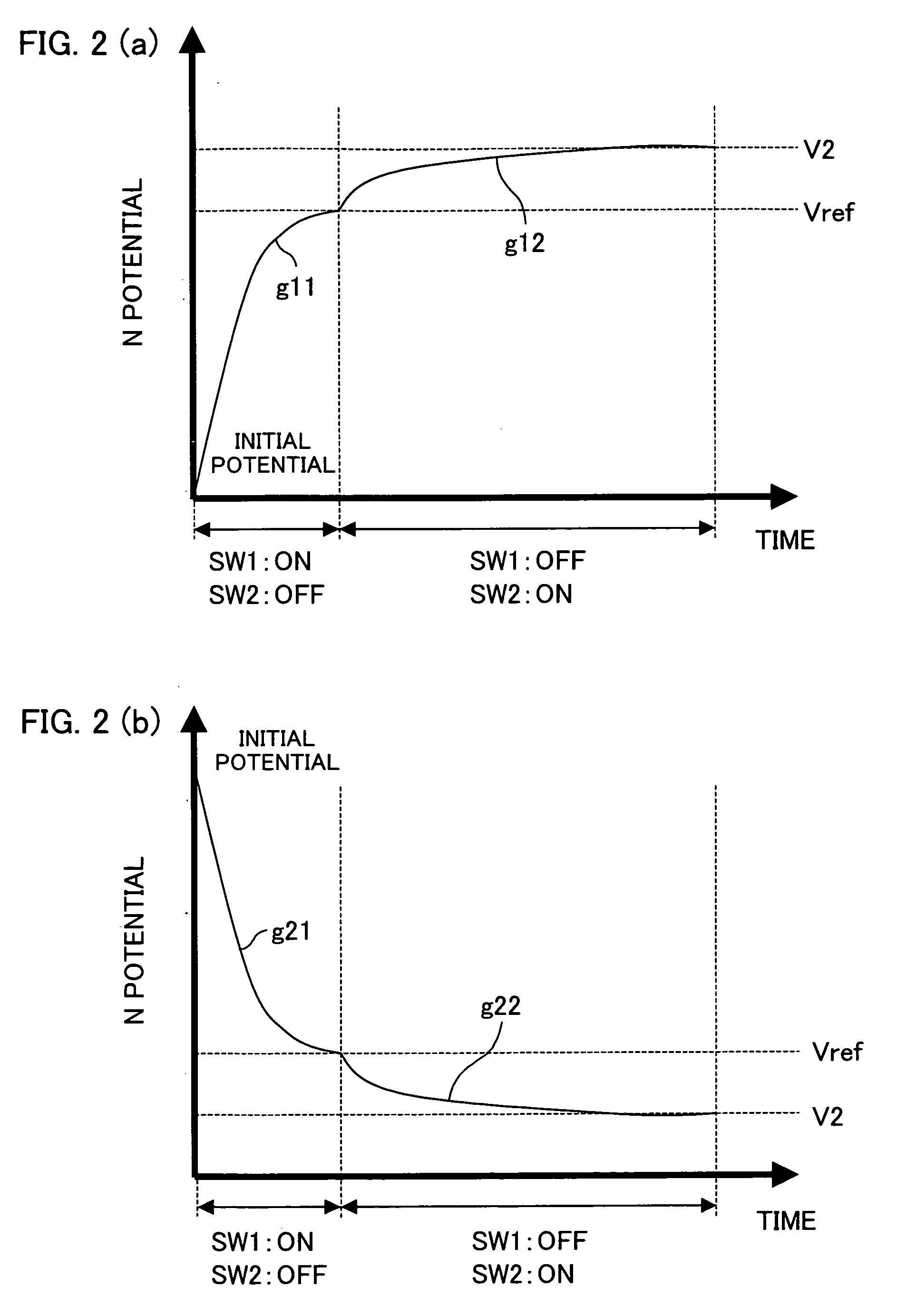
advantage that power is less consumed than that of the aforementioned analog output circuit. However, depending on a relation of (i) a charge time (Tch) taken to charge the load via the TFT of the switch element and (ii) a
response time (Tres) required in driving the switch TFT in accordance with a result of comparison between a load potential and a predetermined reference potential, a final writing potential is determined. Thus, if the relation is such that Tch≦Tres, the load is excessively charged so that the excess at least corresponds to a value indicated by Tres−Tch. If the relation is such that Tch>>Tres, it is impossible to charge the load at high speed.
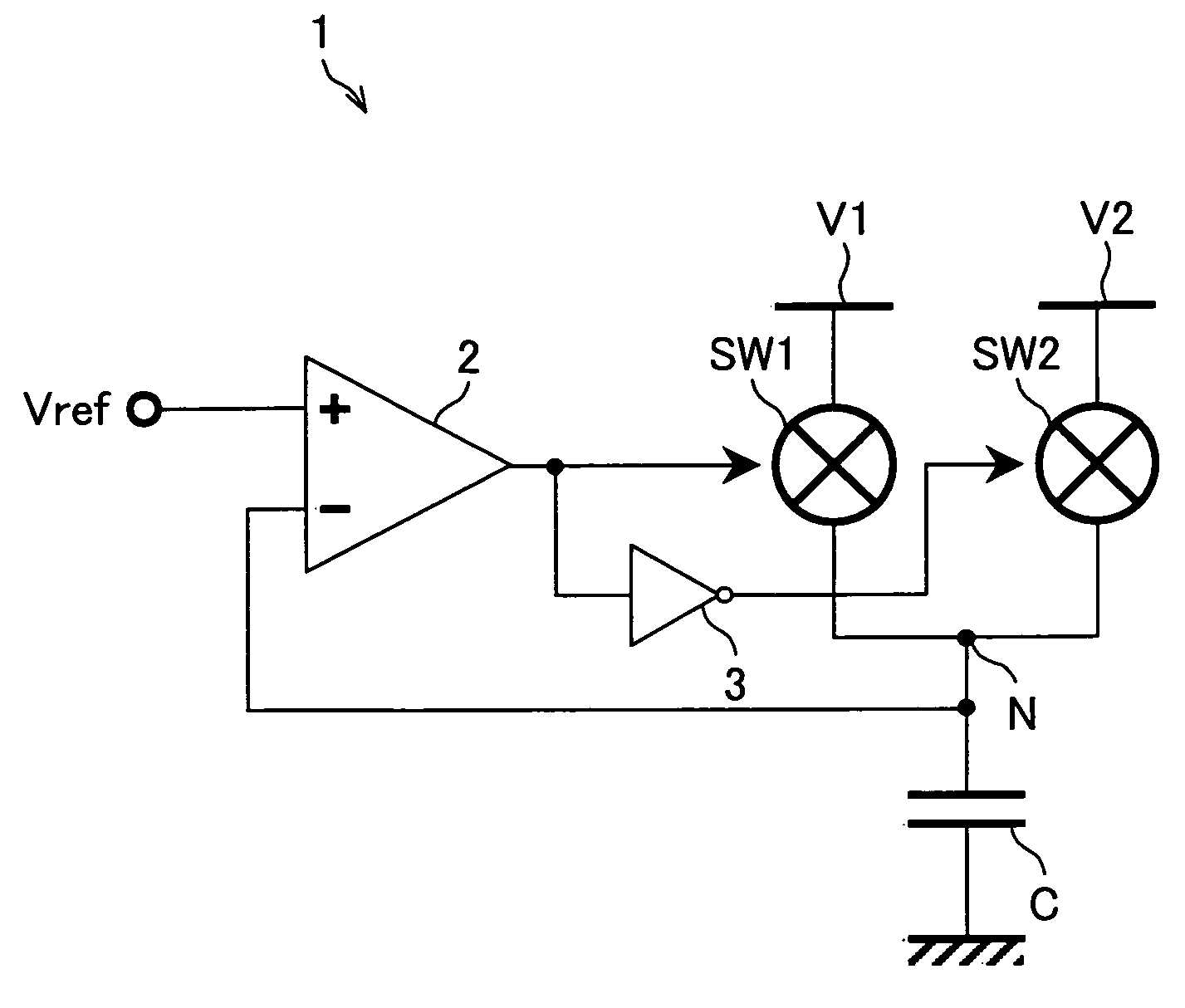
[0045]The present invention was made in view of the foregoing problems, and an object of the present invention is to realize an analog output circuit, a data signal line driving circuit, a display, and a potential writing method, each of which allows a desired potential to be written on a capacitive load with a simple arrangement, low power consumption, high speed, and high accuracy.
[0048]As a result, a potential can be written onto the capacitive load to some extent in a short period by a
voltage source having a lower
output impedance, so that it is possible to suppress power consumption in the
voltage source. Further, after writing a potential by a voltage source having a lower output impedance, a potential is written by a voltage source having a higher output impedance, so that it is possible to carry out the writing with high accuracy by causing a voltage source which has a higher output impedance and hardly generates an offset to write a potential so that the potential of the capacitive load attains the predetermined potential even if an offset occurs in an output of a voltage source having a lower output impedance. Further, the writing is carried out to some extent by the voltage source having a lower output impedance, so that it does not take so long time for the voltage source having a higher output impedance to write the potential. Further, in writing a potential, switch elements are changed so as to sequentially switch voltage sources used for the writing, so that it is easy to carry out the writing and a writing rate depends only on a writing
time constant and a rate in changing the switch elements. Thus, the writing can be carried out at high speed as a whole.
[0049]In this manner, it is possible to realize an analog output circuit which can write a desired potential onto the capacitive load with a simple arrangement, low power consumption, high speed, and high accuracy.

