Liquid crystal display device, manufacturing method thereof, and electronic apparatus

a technology of liquid crystal display device and manufacturing method, which is applied in the direction of liquid surface applicators, coatings, instruments, etc., can solve the problems of increasing the number of processes and the manufacturing cost, increasing the thickness of the liquid crystal display device, and not being able to achieve the effect of reducing the thickness

Inactive Publication Date: 2009-07-09
SEIKO EPSON CORP
View PDF6 Cites 6 Cited by
  • Summary
  • Abstract
  • Description
  • Claims
  • Application Information

AI Technical Summary

Benefits of technology

[0066]In the third aspect of the invention, it is possible to precisely form at least one of the first transparent thin film and the second transparent thin film with a regular thickness having uniformity.

Problems solved by technology

However, the above-described prior art has the following problems.
A color filter layer provided for each pixel by using a predetermined colorant causes an increase in the number of processes and in the manufacturing cost.
In addition, since the color filter layer is provided, the thickness of the liquid crystal display device increases, and there is a problem in that a reduction of the thickness is not easily realized.

Method used


Image

  • Liquid crystal display device, manufacturing method thereof, and electronic apparatus
  • Liquid crystal display device, manufacturing method thereof, and electronic apparatus
  • Liquid crystal display device, manufacturing method thereof, and electronic apparatus

Examples


first embodiment

[0125]Next, a first embodiment of the reference color developing sections and a manufacturing method thereof will be described with reference to FIG. 4.

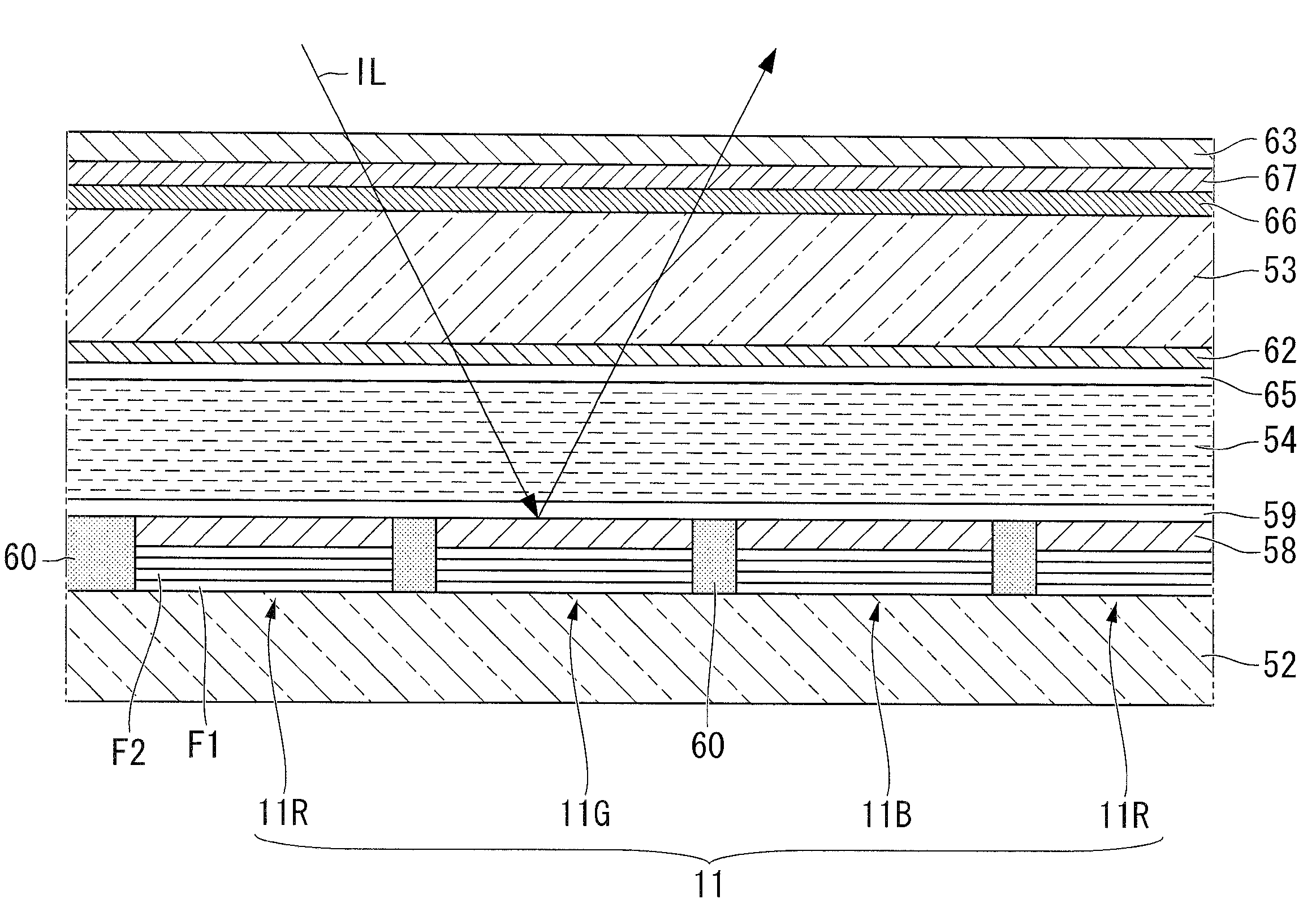
[0126]As shown in FIG. 4, each of the reference color developing sections 11R, 11G, and 11B is formed by alternately forming a plurality of first transparent thin films F1 and a plurality of second transparent thin films F2 having different refractive indexes.

[0127]In the first embodiment, in order from the lower substrate 52, the first transparent thin films F1 are formed in odd-numbered layers such as a first layer, a third layer, . . . , to an eleventh layer. Also, the second transparent thin films F2 are formed in even-numbered layers such as a second layer, . . . , to a tenth layer. Therefore, each of the reference color developing sections 11R, 11G, and 11B is formed by the eleven-layer thin films.

[0128]As a material for forming the first transparent thin film F1 and the second transparent thin film F2, polysiloxane resin (refr...

example

[0139]A first transparent thin film F1 and a second transparent thin film F2 were formed using a first liquid material including a siloxane polymer (refractive index 1.42) as the first transparent thin film F1 and using a second liquid material including a titanium oxide (refractive index 2.52) as the second transparent thin film F2.

[0140]For example, to produce a blue color (λ=480 nm), the first transparent thin film F1 was formed with a thickness t1 of 84.5 nm and the second transparent thin film F2 was formed with a thickness t2 of 47.6 nm, on the basis of the formula (3).

[0141]As a result, as shown in FIG. 5A, it is possible to obtain blue color developing characteristics at a reflectance that is greater than or equal to 80%.

[0142]Similarly, for example, to produce a green color (λ=520 nm), the first transparent thin film F1 was formed with a thickness t1 of 91.5 nm and the second transparent thin film F2 was formed with a thickness t2 of 52.0 nm, on the basis of the formula (3)...

second embodiment

[0151]Next, a second embodiment of the reference color developing sections and a manufacturing method thereof will be described with reference to FIG. 6. Therefore, in FIG. 6, identical symbols are used for the elements which are identical to those of the above-described embodiment shown in FIGS. 1 to 5C, and the explanations thereof are omitted or simplified.

[0152]As shown in FIG. 6, in the reference color developing sections 11R, 11G, and 11B according to the second embodiment, a plurality of granular members 70 functions as an irregularity formation section that forms an irregularity on a front face (first face) of a multilayered interference film in which the first transparent thin films F1 and the second transparent thin films F2 are stacked in layers (herein, only the two layers are shown in FIG. 6 for the convenience), are distributed with intervals at a portion which is close to a back face (second face) of the multilayered interference film.

[0153]The granular members 70 are...


PUM

PropertyMeasurementUnit
thickness t2aaaaaaaaaa
reflectanceaaaaaaaaaa

Abstract

A liquid crystal display device, includes: a liquid crystal layer; and a color developing section that has a multilayered interference film in which first transparent thin films and second transparent thin films are alternatively stacked in layers, and causes light passed through the liquid crystal layer to have predetermined color developing characteristics and to be emitted from the color developing section, each of the first transparent thin films being formed with a first formation material and having a first refractive index so that each of the first transparent thin films has a thickness determined based on the predetermined color developing characteristics, and each of the second transparent thin films being formed with a second formation material and having a second refractive index so that each of the second transparent thin films has a thickness determined based on the predetermined color developing characteristics.

Description

CROSS-REFERENCE TO RELATED APPLICATION[0001]This application is based on and claims priority from Japanese Patent Application No. 2008-001457, filed on Jan. 8, 2008, the contents of which are incorporated herein by reference.BACKGROUND[0002]1. Technical Field[0003]The present invention relates to a liquid crystal display device, a manufacturing method thereof, and an electronic apparatus.[0004]2. Related Art[0005]Semi-transmission reflective types of liquid crystal display devices provided with a transmissive mode and a reflective mode have been known as a liquid crystal display device. As such a semi-transmission reflective type of liquid crystal display devices, there is proposed a liquid crystal display device in which a liquid crystal layer is held in between an upper substrate and a lower substrate, an inner surface of the lower substrate is provided with a reflection film having a light transmitting window formed on a metal film such as aluminum, and the reflection film functi...

Claims


Application Information

Patent Timeline
Patent Type & Authority Applications(United States)
IPC IPC(8): G02F1/1335G02F1/13
CPCB41J2/14233B41J2202/09G02F2001/133521G02F1/133516G02F1/1303G02F1/133521B05C5/00G02F1/13G02F1/1335
Inventor TAKANO, YASUSHIHIRAI, TOSHIMITSU
Owner SEIKO EPSON CORP
Why Eureka
Try Eureka