Chemical mechanical polishing slurry and semiconductor device manufacturing method
a technology of mechanical polishing slurry and manufacturing method, which is applied in the direction of manufacturing tools, lapping machines, other chemical processes, etc., can solve the problems of deteriorating the electric characteristics of wiring
- Summary
- Abstract
- Description
- Claims
- Application Information
AI Technical Summary
Benefits of technology
Problems solved by technology
Method used
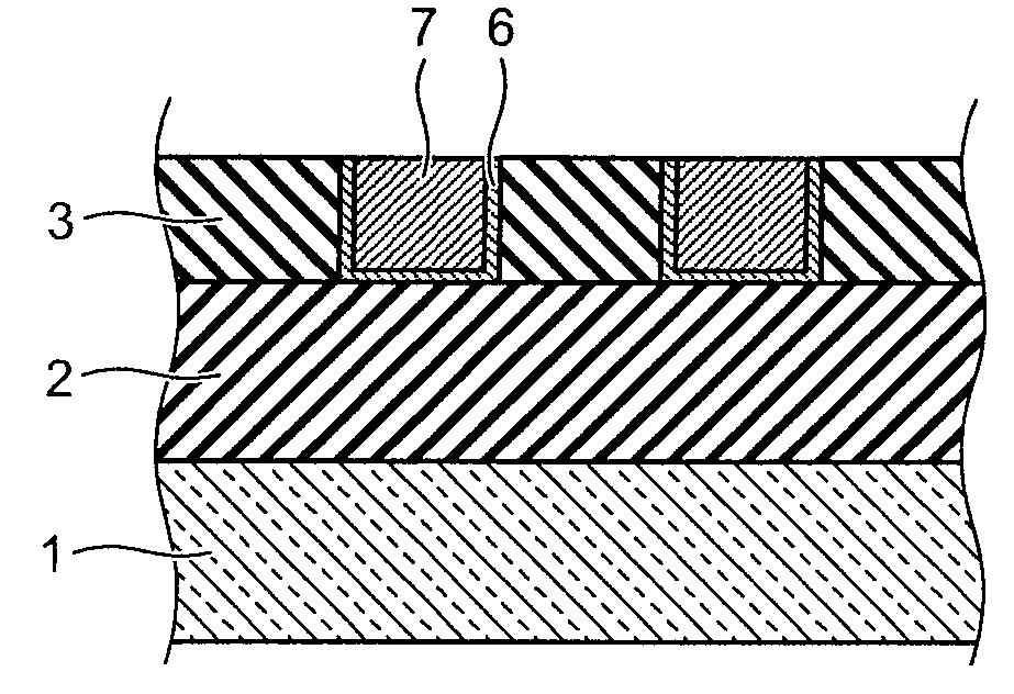
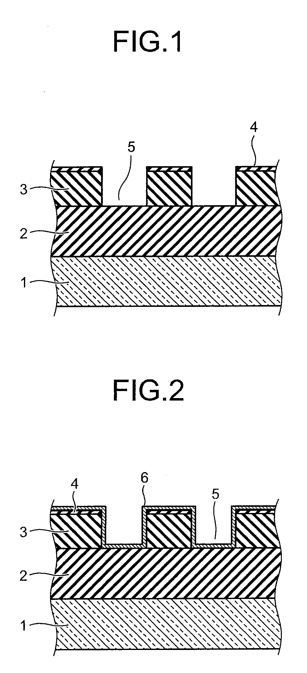
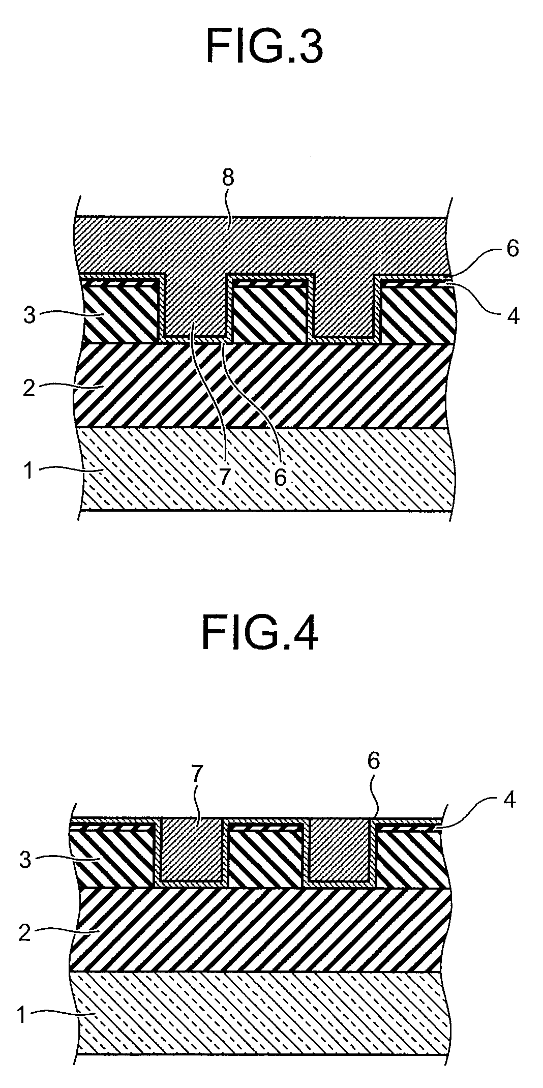
Image

Examples
examples
Examples of the present invention are explained below
[0052]Note that the following Examples are only illustrative and should not be construed as a limitation on the present invention.
examples 1 to 5
[0053]The first CMP slurry used in the first CMP process was prepared according to the components and compounding ratio shown in Table 1 below, and the first CMP slurry was used as the first CMP slurry commonly in Examples 1 to 5.
TABLE 1Composition of the first CMP slurryComponentsContent (mass %)WaterBalanceWater-insolubleQuinaldinic acid0.3Cu complex-Quinolinic acid0.3forming agentWater-soluble CuAlanine0.3complex-formingOxalic acid0.1agentOxidizing agentAmmonium2.5persulfateSurfactantPotassium0.03dodecylbenzenesulfonatePolyvinyl0.03pyrrolidoneAbrasive grainColloidal silica0.75pH adjustingKOH(Adjusted to pH 9)agent
[0054]The second CMP slurry used in the second CMP process in each of the Examples 1 to 5 was prepared according to the components and compounding ratio shown in Table 2 below.
PUM
| Property | Measurement | Unit |
|---|---|---|
| particle size | aaaaa | aaaaa |
| particle size | aaaaa | aaaaa |
| particle size | aaaaa | aaaaa |
Abstract
Description
Claims
Application Information
 - R&D Engineer
- R&D Manager
- IP Professional
- Industry Leading Data Capabilities
- Powerful AI technology
- Patent DNA Extraction
Browse by: Latest US Patents, China's latest patents, Technical Efficacy Thesaurus, Application Domain, Technology Topic.
© 2024 PatSnap. All rights reserved.Legal|Privacy policy|Modern Slavery Act Transparency Statement|Sitemap